Why Understanding PCB Cost Matters
PCB manufacturing costs range from under $10 for simple 2-layer prototypes to over $1,000 for complex multilayer HDI boards. Understanding what drives these costs enables smarter design decisions, more accurate budget planning, and more effective supplier negotiations. Engineers who grasp cost drivers can optimize designs for budget without sacrificing the quality their applications require.
The global PCB market exceeds $60 billion annually, with prices varying dramatically based on specifications, volume, and supplier. A design that costs $500 per board in prototype quantities might cost $50 per board at 10,000 pieces. Similarly, a design using specialized materials might cost five times more than one using standard FR-4. Without understanding these relationships, engineers risk budget overruns, delayed projects, and poor supplier relationships.
This guide breaks down PCB manufacturing costs into understandable components, explains the factors that drive each cost element, and provides strategies for optimizing your designs to meet budget targets.
Cost Breakdown: Layer Count
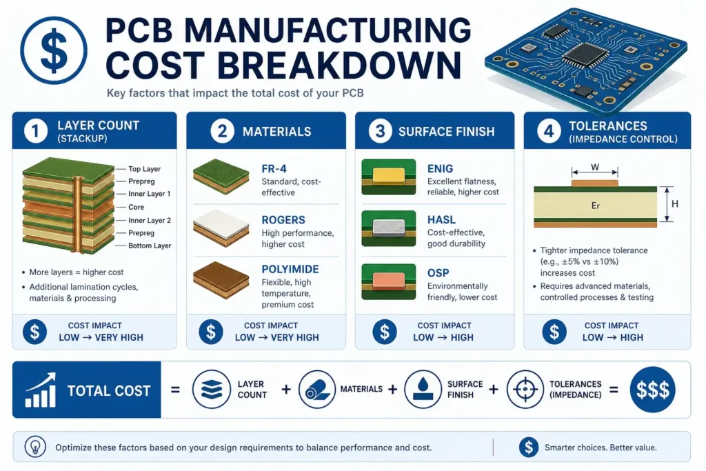
Layer count is typically the single largest cost driver for multilayer boards. Each additional layer requires additional processing steps: inner layer imaging, etching, oxide treatment, lamination, drilling, plating, and final finishing. The cost increase per additional layer varies by manufacturer but typically ranges from 15-30% per layer.
| Layer Count | Relative Cost Index | Typical Use |
|---|---|---|
| 2-layer | 1.0x (baseline) | Simple designs, cost-sensitive applications |
| 4-layer | 2-3x | Most common multilayer, moderate complexity |
| 6-layer | 4-6x | High-speed designs, complex routing |
| 8-layer | 6-10x | Advanced applications, tight routing density |
| 10+ layer | 10-20x | Complex HDI, military, aerospace |
Reducing layer count where possible is the most effective cost optimization strategy. Often, a well-designed 4-layer board can accommodate functionality that initially seemed to require 6 layers.
Cost Breakdown: Board Size and Panel Utilization
PCB manufacturers produce boards on standard panel sizes—typically 18×24 inches or 21×25 inches. Your board’s size determines how many boards fit on each panel, directly affecting per-board cost. Better panel utilization means lower per-board cost.
Designs that use nearly the full panel are most economical. Boards smaller than 2×2 inches may incur minimum charge penalties. Irregular board shapes that don’t nest efficiently waste panel space. Work with your manufacturer to optimize board size and panelization for your quantity requirements.
Panel utilization optimization strategies include:
- Panelization: Arraying multiple boards together for production
- Nesting: Arranging boards to minimize wasted space
- Standard sizes: Using common dimensions that fit standard panels
- Score vs. punch: Choosing manufacturing methods that maximize yield
Cost Breakdown: Material Selection
Material cost represents 15-40% of total PCB cost, varying by board type. Standard FR-4 epoxy glass is the most economical option for most applications. Specialized materials command significant premiums.
| Material | Cost Level | Multiplier vs FR-4 | Typical Applications |
|---|---|---|---|
| Standard FR-4 | Low | 1.0x | General purpose, consumer electronics |
| High-Tg FR-4 | Low-Medium | 1.1-1.3x | Lead-free assembly, thermal resistance |
| Mid-Loss FR-4 | Medium | 1.3-1.8x | Moderate speed, cost-sensitive high-frequency |
| Low-Loss (Megtron 6) | High | 3-5x | High-speed digital (10+ Gbps) |
| Ultra-Low-Loss (Megtron 7) | Very High | 5-8x | Ultra-high-speed, RF |
| Rogers RT/duroid | Very High | 5-10x | RF/microwave applications |
| Polyimide | High | 2-4x | High-temperature, flexible applications |
| Aluminum Core | Medium-High | 1.5-3x | LED, thermal management |
Use specialized materials only when your application genuinely requires their properties. High-speed materials for a 100 Mbps interface waste budget; they’re only necessary for multi-Gbps applications.
Cost Breakdown: Surface Finish
Surface finish affects both cost and board functionality. The finish protects copper pads, enables soldering, and affects assembly reliability. Different finishes offer different trade-offs between cost, shelf life, and performance.
| Finish | Cost Level | Relative Cost | Shelf Life |
|---|---|---|---|
| HASL (Leaded) | Lowest | 1.0x | Indefinite |
| HASL Lead-Free | Low | 1.1-1.2x | Indefinite |
| OSP | Low-Medium | 1.0-1.3x | 6-12 months |
| Immersion Silver | Medium | 1.2-1.5x | 12-18 months |
| ENIG | Medium-High | 1.5-2.0x | 24+ months |
| ENEPIG | High | 2.0-3.0x | 24+ months |
| Hard Gold | Highest | 3.0-10x | Indefinite |
For most applications, ENIG offers the best balance of cost, shelf life, and performance. HASL remains popular for through-hole assemblies where coplanarity isn’t critical.
Cost Breakdown: Tolerance Requirements
Tighter tolerances require more precise manufacturing processes, more frequent inspection, and often more experienced operators. The cost impact varies by tolerance type:
Impedance Tolerance:
- Standard ±10%: Minimal cost impact
- Tight ±5%: 20-40% cost increase, specialized processing required
- Ultra-tight ±3%: 50-100% cost increase, limited manufacturers
Dimensional Tolerances:
- Standard IPC Class 2: Baseline cost
- Tight IPC Class 3: 15-25% cost increase
- Custom tolerances: Varies by specification
Trace/Space Tolerances:
- Standard 4-6 mil: Baseline cost
- Fine line 2-4 mil: 20-40% cost increase
- Ultra-fine <2 mil: 50-100% cost increase
Only specify tolerances that your application genuinely requires. A ±10% impedance tolerance is fine for USB 2.0 but inadequate for PCIe Gen 4.
Cost Breakdown: Copper Weight
Copper weight affects current capacity, trace heating, and manufacturing complexity. Standard copper weights are 0.5 oz, 1 oz, and 2 oz per square foot. Heavier copper requires longer etching time and affects minimum trace/space capabilities.
| Copper Weight | Thickness | Cost Impact | Applications |
|---|---|---|---|
| 0.5 oz (H/H) | 0.7 mil | Baseline | Fine line, high-density designs |
| 1 oz (1/1) | 1.4 mil | 1.0-1.1x | Most common, controlled impedance |
| 2 oz (2/2) | 2.8 mil | 1.2-1.5x | Power distribution, high current |
| 3 oz+ | 4.2+ mil | 1.5-2.0x | Heavy power applications |
Heavy copper boards require longer etching time, which increases cost and can affect fine feature capability. Specify only the copper weight your application requires.
Volume Pricing Tiers
PCB manufacturing exhibits strong economies of scale. Understanding volume tiers helps with cost planning:
| Quantity | Typical Price Reduction | Best For |
|---|---|---|
| 1-5 pieces | Baseline (highest) | Prototyping, engineering validation |
| 5-20 pieces | 10-20% | Design verification |
| 20-100 pieces | 20-40% | Pilot production, small series |
| 100-500 pieces | 40-60% | Low-volume production |
| 500+ pieces | 60-80% | Mass production |
At high volumes, panel utilization optimization, automated handling, and process efficiencies drive cost reductions. Prototype pricing often includes significant setup cost amortization.
Hidden Cost Factors
Beyond obvious specifications, several hidden factors affect PCB cost:
Tooling and Setup: Every PCB order incurs setup costs regardless of quantity. These costs include engineering review, film generation, drill file preparation, and machine setup. Setup costs are amortized across the order quantity, so larger orders have lower per-board setup costs.
Testing and Inspection: Electrical testing—flying probe or bed-of-nails—adds cost but catches manufacturing defects. Automated Optical Inspection (AOI) and X-ray inspection for complex boards add further cost.
Documentation and Certifications: Military, medical, and automotive applications require additional documentation, process controls, and certifications:
- ITAR compliance: 10-30% cost increase
- AS9100/ISO 9001 certified manufacturing: 10-20% cost increase
- MIL-PRF-31032 qualification: 50-100% cost increase
Expedited Services: Rush orders typically incur premium pricing:
- 24-hour turnaround: 2-5x standard price
- 48-72 hour turnaround: 1.5-3x standard price
- 1-week standard: Baseline pricing
Cost Reduction Strategies
Design Optimization
Design decisions made early in the development process have the greatest cost impact:
- Right-size layer count: Each layer adds cost; optimize routing to minimize layers
- Standardize materials: Use common materials across products where possible
- Relax tolerances: Specify only necessary tolerances; ±10% costs less than ±5%
- Optimize panel utilization: Size boards to fit efficiently on standard panels
- Consider standard finishes: ENIG is versatile; reserve expensive finishes for justified cases
Manufacturing Optimization
Working with your manufacturer can reduce costs:
- Early engagement: Involve manufacturer in design phase for DFM feedback
- Design for their capabilities: Learn their standard processes and design within them
- Standardize stack-ups: Use common configurations across product lines
- Share volume: Combining similar orders reduces per-board cost
- Build relationships: Long-term partnerships often receive better pricing
Supply Chain Optimization
Strategic sourcing reduces costs:
- Compare multiple quotes: Prices vary significantly between manufacturers
- Consider offshore manufacturing: May offer 30-50% cost savings with longer lead times
- Balance cost vs. risk: Lowest cost isn’t always best; consider reliability and lead time
- Consolidate suppliers: Volume with fewer suppliers often earns better pricing
- Plan ahead: Longer lead times often enable more economical production
Quote Comparison Guide
Comparing PCB quotes requires careful attention to ensure apples-to-apples comparison:
What to Verify in Each Quote:
- Specifications match: Confirm all parameters—dimensions, layers, materials, tolerances, finish—are identical
- Quantities: Verify order quantities match your request
- Lead times: Note standard vs. expedited pricing
- Included services: Testing, AOI, documentation, inspection
- Payment terms: Net 30 vs. Net 60 affects pricing
- Tooling/fixture costs: Some quotes amortize tooling; others charge separately
Red Flags in Quotes:
Be cautious of quotes that seem too low:
- Price significantly below market average may indicate quality shortcuts
- Missing specifications may mean unfavorable defaults
- No testing included may mean untested boards
- Unverified manufacturers may lack quality systems
Requesting Clarification:
Ask manufacturers to clarify:
- Material brand names and specifications
- Stack-up details and layer assignments
- Testing procedures and coverage
- Inspection methods and acceptance criteria
- Documentation provided with shipment
Frequently Asked Questions
What is the typical cost range for PCB manufacturing?
Simple 2-layer prototypes typically cost $5-50 depending on specifications and quantity. 4-layer prototypes range from $50-200. 6-layer and higher prototypes cost $100-500 or more. Production quantities reduce per-board cost by 40-80% depending on volume. Complex multilayer, HDI, and flexible boards cost significantly more.
What specification affects PCB cost the most?
Layer count is typically the highest-impact cost driver for multilayer boards. A 6-layer board costs 4-6x more than an equivalent 2-layer board. Board size and panel utilization are close seconds, especially for small quantities. Material selection and tolerance requirements also significantly affect cost.
How can I reduce PCB manufacturing costs?
Design optimization offers the greatest cost reduction opportunity: reduce layer count, use standard materials, relax tolerances, and optimize board size for panel utilization. On the supply side, compare multiple quotes, build manufacturer relationships, and plan orders to maximize volume pricing. Consider standard finishes and avoid specialized requirements unless necessary.
Why do prototype PCBs cost more per unit than production?
Prototype pricing reflects setup costs amortized over fewer boards. Engineering review, tooling preparation, and process setup take similar time regardless of quantity. Small prototype quantities also mean poor panel utilization. Production orders spread these costs across many boards, reducing per-board cost significantly.
How do I compare quotes from different manufacturers?
Ensure all quotes specify identical specifications: dimensions, layers, material, thickness, tolerances, surface finish, color, and testing requirements. Verify quantities match. Compare included services—testing, inspection, documentation—between quotes. Consider lead time, payment terms, and manufacturer reputation, not just price.
When should I use specialized PCB materials?
Specialized materials—high-speed, RF, polyimide—are necessary when your application requires their specific properties: low loss at high frequencies, controlled dielectric constant, high temperature capability, or flexibility. Using Megtron 6 for a 100 Mbps interface wastes budget; standard FR-4 handles those signals adequately. Reserve specialized materials for applications that genuinely need them.
References
- IPC-2221: Generic Standard on Printed Circuit Board Design
https://www.ipc.org/ - IPC-4101: Specification for Base Materials for Rigid and Multilayer Printed Boards
https://www.ipc.org/ - SMTA: Surface Mount Technology Association Technical Resources
https://www.smta.org/ - Ucamco: Gerber Format Specification
https://www.ucamco.com/en/gerber
Further Reading
- Custom PCB Manufacturer — Finding suppliers for your cost requirements
- PCB Prototype Manufacturing — Optimizing prototype costs
- Quick-Turn PCB Prototype — Expedited services and premiums
- Low-Volume PCB Manufacturing — Strategies for small batch production
- Multilayer PCB Manufacturer — Multilayer cost factors
- PCB Quote Requirements — Documentation for accurate quotes
- PCB Surface Finish Comparison — Finish cost comparison
Shanghai Huangte Technology Co., Ltd. | Last updated: 2026-07-25
This article provides general guidance on PCB manufacturing costs. Actual costs vary by manufacturer, region, specifications, and market conditions. Always request detailed quotes with full specification breakdowns for accurate pricing.