What Is a Multilayer PCB Manufacturer?
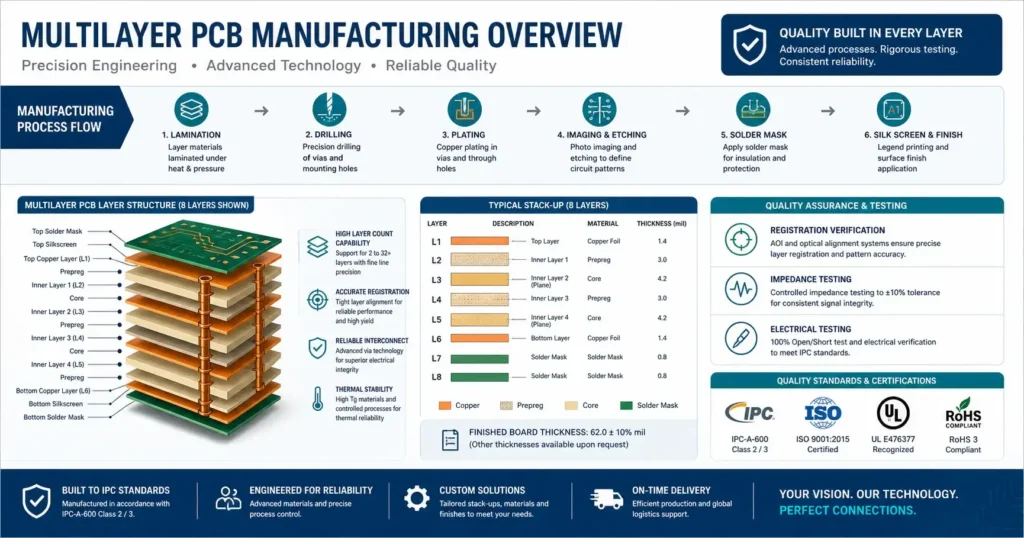
A multilayer PCB manufacturer specializes in producing printed circuit boards with four or more conductive layers, where signal and power planes are distributed across internal layers. Unlike single-sided or double-sided boards, multilayer boards require lamination cycles to bond inner layers together, precision drilling to connect layers through plated through-holes, and rigorous registration control to maintain alignment across all layers.
In 2026, multilayer PCB fabrication spans layer counts from 4 to 40+ layers, with 4-layer, 6-layer, and 8-layer boards representing the majority of commercial applications. Higher layer counts (12, 16, 24, 32+ layers) serve telecommunications infrastructure, data center equipment, aerospace systems, and advanced computing applications where signal integrity and power distribution requirements exceed what lower layer counts can efficiently provide.
The manufacturing complexity increases non-linearly with layer count. A 4-layer board requires one lamination cycle and one drill operation. An 8-layer board may require two lamination cycles (for buried vias), multiple drill operations with different drill programs, and more complex electrical testing. A 16+ layer board involves sequential lamination, blind and buried via structures, impedance-controlled routing, and extensive cross-section analysis to verify layer integrity.
Stack-Up Verification: What the Manufacturer Must Deliver
The board stack-up—the specific combination of core thicknesses, prepreg materials, and copper weights arranged in a defined sequence—is the foundation of multilayer PCB manufacturing. A qualified multilayer PCB manufacturer must provide stack-up documentation that specifies each dielectric layer’s material and thickness, each copper layer’s weight (base copper and finished copper after plating), and the overall finished board thickness and tolerance.
Pre-engineered stack-ups offer faster quoting and production because the manufacturer has already validated the material combinations, lamination parameters, and expected impedance ranges. Manufacturers typically offer standard stack-ups for common configurations: 4-layer boards with 1.2mm or 1.6mm total thickness, 6-layer boards with symmetric or asymmetric configurations, and 8-layer boards with defined spread and power plane locations.
Custom stack-ups become necessary when the application requires specific impedance targets that standard stack-ups cannot achieve, non-standard total thickness, specialized materials (high-Tg, low-loss, Rogers high-frequency laminates), or thermal management features such as heavy copper internal planes.
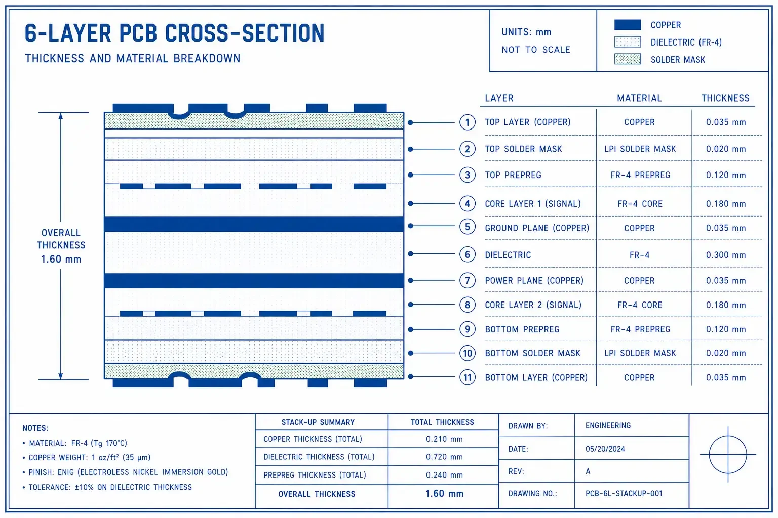
When requesting a custom stack-up, provide the manufacturer with target impedance values and tolerances, required signal layer positions, power and ground plane locations, total thickness constraints from the enclosure, and thermal requirements. The manufacturer should return a proposed stack-up diagram showing layer sequence, dielectric materials and thicknesses, copper weights, and expected impedance ranges for controlled impedance traces.
Registration and Tolerance Control
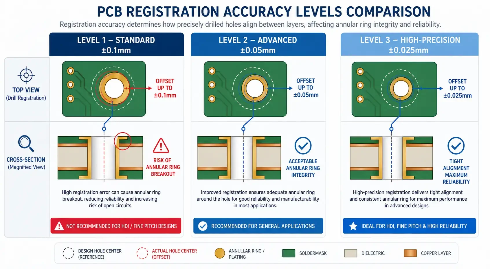
Layer-to-layer registration—how accurately the inner layer patterns align with each other and with the drilled hole pattern—is the single most critical process metric in multilayer fabrication. Registration error manifests as annular ring breakout: the drill hole misses the target pad because the inner layer image shifted during lamination. Even partial breakout creates reliability risk.
Advanced multilayer PCB manufacturers maintain registration tolerance of ±0.05mm (2 mil) or better across the panel. This tolerance accounts for inner layer imaging accuracy, lamination press uniformity, drill registration, and cumulative tolerance buildup across all layers. Registration capability is verified through coupon testing and cross-section analysis.
Annular ring design must accommodate registration tolerance while maintaining reliable plating coverage. IPC-6012 specifies minimum annular ring requirements based on hole size and IPC class level. For Class 3 boards with 0.35mm diameter holes, a minimum finished pad diameter of 0.55mm (annular ring of 0.10mm) is typically required. Design rules should target annular rings of 0.125mm (5 mil) or larger where layout permits.
Drill-to-copper clearance—the space between the drill hit and adjacent traces on inner layers—requires careful attention in multilayer designs. The manufacturer’s design rules typically specify minimum drill-to-copper spacing that prevents drilling damage to adjacent copper features. This clearance may constrain fine-pitch BGA routing and high-density interconnect areas.
Controlled Impedance Requirements
Controlled impedance PCBs require the manufacturer to verify that trace impedance stays within specified tolerance across manufacturing variation. This verification requires test coupons—additional board structures fabricated alongside the production boards that contain impedance test traces matching the production board’s impedance-controlled lines.
Test coupons must replicate the same layer position, trace width, trace thickness, dielectric material, and dielectric thickness as the production traces they represent. Coupon placement within the production panel must be documented so that impedance measurements can be correlated to production boards.
Time Domain Reflectometry (TDR) is the standard measurement method for impedance verification. TDR instruments launch a fast-rise-time pulse into the trace and measure the reflected signal to calculate characteristic impedance. A qualified manufacturer maintains calibrated TDR equipment and provides impedance test reports showing measured values for each coupon trace type.
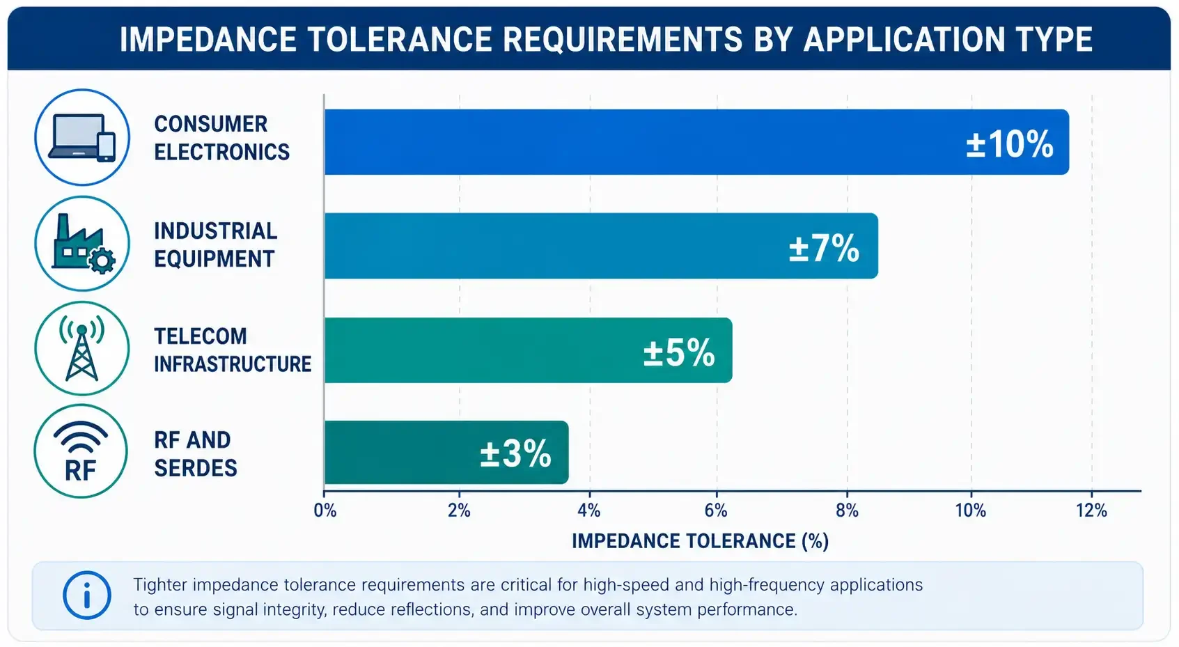
Impedance tolerance depends on the application. Standard tolerance of ±10% covers most commercial applications. Tighter tolerance of ±5% or ±3% is required for high-speed digital interfaces (DDR5, PCIe Gen5, 112G SerDes), RF applications, and precision analog circuits. Specify the tolerance your application requires rather than defaulting to tighter tolerances that increase cost without benefit.
Quality Certifications and Standards
IPC standards define the qualification and performance requirements for multilayer PCBs. IPC-6012, “Qualification and Performance Specification for Rigid Printed Boards,” is the primary specification for multilayer board qualification. It defines three class levels:
- Class 1 (General Electronic Products): Consumer electronics where functional performance is the primary concern
- Class 2 (Dedicated Service Electronic Products): Commercial and industrial equipment with extended life requirements
- Class 3 (High-Performance/Harsh Environment Electronic Products): Aerospace, medical, military, and automotive safety applications where continued performance is critical
IPC-A-600, “Acceptability of Printed Boards,” defines visual acceptance criteria for all three class levels. The manufacturer should maintain current IPC certification for their quality inspectors and process operators.
ISO 9001 certification indicates the manufacturer has implemented a documented quality management system covering process control, incoming material inspection, in-process quality checks, final inspection, nonconformance handling, and corrective action. While ISO 9001 alone does not guarantee PCB fabrication competence, it indicates a structured approach to quality management.
UL 94 V-0 certification verifies the board’s flame retardant properties. Most commercial and industrial applications require boards to meet UL 94 V-0 flame rating. The UL mark on the board indicates the manufacturer holds a UL product authorization for that specific board construction.
For defense and aerospace applications, ITAR (International Traffic in Arms Regulations) compliance may be required. Verify the manufacturer’s ITAR registration and export control procedures if your application involves defense-related electronics.
Supplier Evaluation Checklist
Evaluating multilayer PCB manufacturers requires systematic assessment across multiple dimensions.
Technical Capability Matrix
Request a capability matrix documenting maximum layer count, minimum trace width and spacing, minimum drill diameter, maximum aspect ratio (board thickness / minimum drill diameter), controlled impedance capability and tolerance range, and available materials (standard FR-4, high-Tg, Rogers, flex).
Sample Evaluation
Request samples of boards similar to your requirements before committing to production. Evaluate registration accuracy through cross-section analysis, impedance consistency across the sample set, drill hole quality and plating uniformity, and solder mask and silkscreen registration.
Process Documentation
Review the manufacturer’s quality manual, process control procedures for critical processes (lamination, drilling, plating), incoming material verification procedures, in-process inspection points, and final test and inspection procedures.
Communication and Responsiveness
Evaluate the manufacturer’s communication quality during the quoting and sample process. Assess response time for technical questions, clarity and completeness of technical communication, and willingness to engage on design for manufacturability feedback.
Frequently Asked Questions
Q1: What layer count do I need for my application?
Layer count requirements depend on circuit complexity, signal integrity requirements, and power distribution needs. A simple microcontroller circuit with 20-30 components may fit on a 4-layer board with two signal layers and two planes. A 32-bit processor with DDR memory interface, power regulators, and multiple peripherals typically requires 6-8 layers. High-speed communications boards (SerDes, optical modules) may require 12-16 layers to manage signal integrity and power distribution complexity. Consult with your manufacturer early in the design phase to validate layer count requirements.
Q2: How do I verify a multilayer manufacturer’s registration accuracy?
Registration accuracy is verified through cross-section analysis. The manufacturer should produce cross-section coupons cut from the production panel that show the drilled hole relative to the internal layer features. Measure the annular ring on all layers—the minimum annular ring must exceed your design requirements. Request cross-section reports as part of your qualification process. Also verify the manufacturer’s registration capability through their documented process capability studies.
Q3: What controlled impedance tolerance should I specify?
The required impedance tolerance depends on your application. For standard digital signals (USB 2.0, Ethernet 100BASE-TX), ±10% tolerance is typically acceptable. For high-speed digital interfaces (USB 3.0, HDMI, DDR4/5 memory), ±7% or ±10% is common. For PCIe Gen5, 112G SerDes, and RF applications, ±5% or tighter may be required. Specify only the tolerance your application actually requires—tighter tolerances increase manufacturing cost and may reduce yield.
Q4: What IPC class should I require for my multilayer PCBs?
Class 2 is appropriate for most commercial and industrial products including consumer electronics, industrial controls, and office equipment. Class 3 is required for aerospace, medical devices, automotive safety systems, and military electronics where board failure has safety implications. Class 1 is acceptable for disposable or short-lifecycle products where board replacement is inexpensive and downtime is acceptable.
Q5: How do I verify multilayer PCB impedance?
Request impedance test coupons as part of your fabrication package. The coupons must match your production board’s impedance-controlled traces in layer position, trace geometry, and dielectric construction. The manufacturer should measure coupons using calibrated TDR equipment and provide a test report showing measured impedance values for each coupon trace type. For critical applications, consider independent verification through a third-party testing laboratory.
References
- IPC-6012: Qualification and Performance Specification for Rigid Printed Boards. IPC.
https://www.ipc.org/ - IPC-A-600: Acceptability of Printed Boards. IPC.
https://www.ipc.org/ - IPC-2221: Generic Standard on Printed Board Design. IPC.
https://www.ipc.org/ - Ucamco. “Gerber Format Specification.”
https://www.ucamco.com/en/gerber - ISO 9001:2015: Quality Management Systems. ISO.
https://www.iso.org/
Further Reading
- Custom PCB Manufacturer: How to Choose the Right Partner for Prototype and Production — Comprehensive guide to evaluating and selecting PCB manufacturers
- PCB Prototype Manufacturing: From Design Files to a Testable Board — Step-by-step prototype manufacturing process
- Quick-Turn PCB Prototypes: What Can Be Fast-Tracked and What Cannot — Expedited multilayer prototype options
- Low-Volume PCB Manufacturing: When a Pilot Run Is Better Than Mass Production — Pilot run decision guide for multilayer production
- PCB Fabrication Process Explained — Detailed breakdown of PCB fabrication stages
Shanghai Huangte Technology Co., Ltd. | Last updated: 2026-07-20
This article is for informational purposes and does not constitute professional engineering or legal advice. Specific PCB requirements should be verified with qualified manufacturers and reviewed by a licensed professional engineer.