What is PCB Copper Weight
PCB copper weight represents the mass of copper coverage per unit area on the board surface, expressed in ounces per square foot (oz/ft²) as the industry standard measurement. This specification describes the copper thickness before processing, including the base copper foil and any subsequent plating added during fabrication. The oz/ft² measurement originates from traditional copper foil production, where one ounce of copper rolled to cover one square foot yields the specified thickness.
Copper weight fundamentally determines the electrical and thermal performance of PCB conductors. Wider traces and heavier copper reduce resistance, enabling higher current flow with lower temperature rise. Conversely, fine-pitch digital circuits may prefer thinner copper to achieve tighter trace geometries for impedance control and routing density. These competing requirements drive copper weight selection based on specific application priorities.
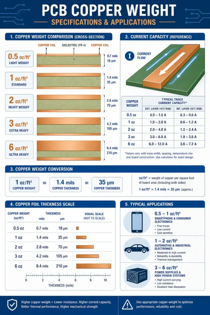
Standard copper weights span a wide range to accommodate diverse requirements. Consumer electronics and mobile devices typically use 0.5 to 1 oz/ft² copper for compact routing and cost optimization. General-purpose industrial and automotive applications commonly specify 1 to 2 oz/ft² for balanced current capacity and manufacturability. Power electronics and motor controls may require 3 to 6 oz/ft² or heavier for significant current handling. The selection process must balance electrical requirements against cost, weight, and manufacturing constraints.
Copper weight terminology in PCB manufacturing distinguishes between base copper and finished copper. Base copper weight refers to the starting foil specification before plating and etching processes. Finished copper weight accounts for plating additions on outer layers and etching reductions, potentially varying from base specifications. Inner layer copper weight specification requires accounting for etch factor compensation to achieve target finished dimensions.
Copper Weight Units Explained
The PCB industry employs multiple units for copper thickness specification, requiring clear understanding for accurate communication with manufacturers. The ounce per square foot (oz/ft²) measurement derives from copper foil manufacturing processes and remains the standard specification format. Converting between units enables cross-reference with design software, material datasheets, and fabrication drawings from different sources.
Standard conversion relationships establish thickness equivalencies across measurement systems. One ounce per square foot corresponds to approximately 1.4 mils (thousandths of an inch), 35 microns (millionths of a meter), or 1.35 thousandths of an inch depending on rounding conventions. These conversions enable designers to interpret specifications from various sources and verify manufacturer capabilities against design requirements.
| Copper Weight | Mils | Microns (μm) | Inches |
|---|---|---|---|
| 0.5 oz/ft² | 0.7 mil | 18 μm | 0.0007″ |
| 1 oz/ft² | 1.4 mil | 35 μm | 0.0014″ |
| 2 oz/ft² | 2.8 mil | 70 μm | 0.0028″ |
| 3 oz/ft² | 4.2 mil | 105 μm | 0.0042″ |
| 4 oz/ft² | 5.6 mil | 140 μm | 0.0056″ |
| 6 oz/ft² | 8.5 mil | 215 μm | 0.0085″ |
| 10 oz/ft² | 14.0 mil | 350 μm | 0.0140″ |
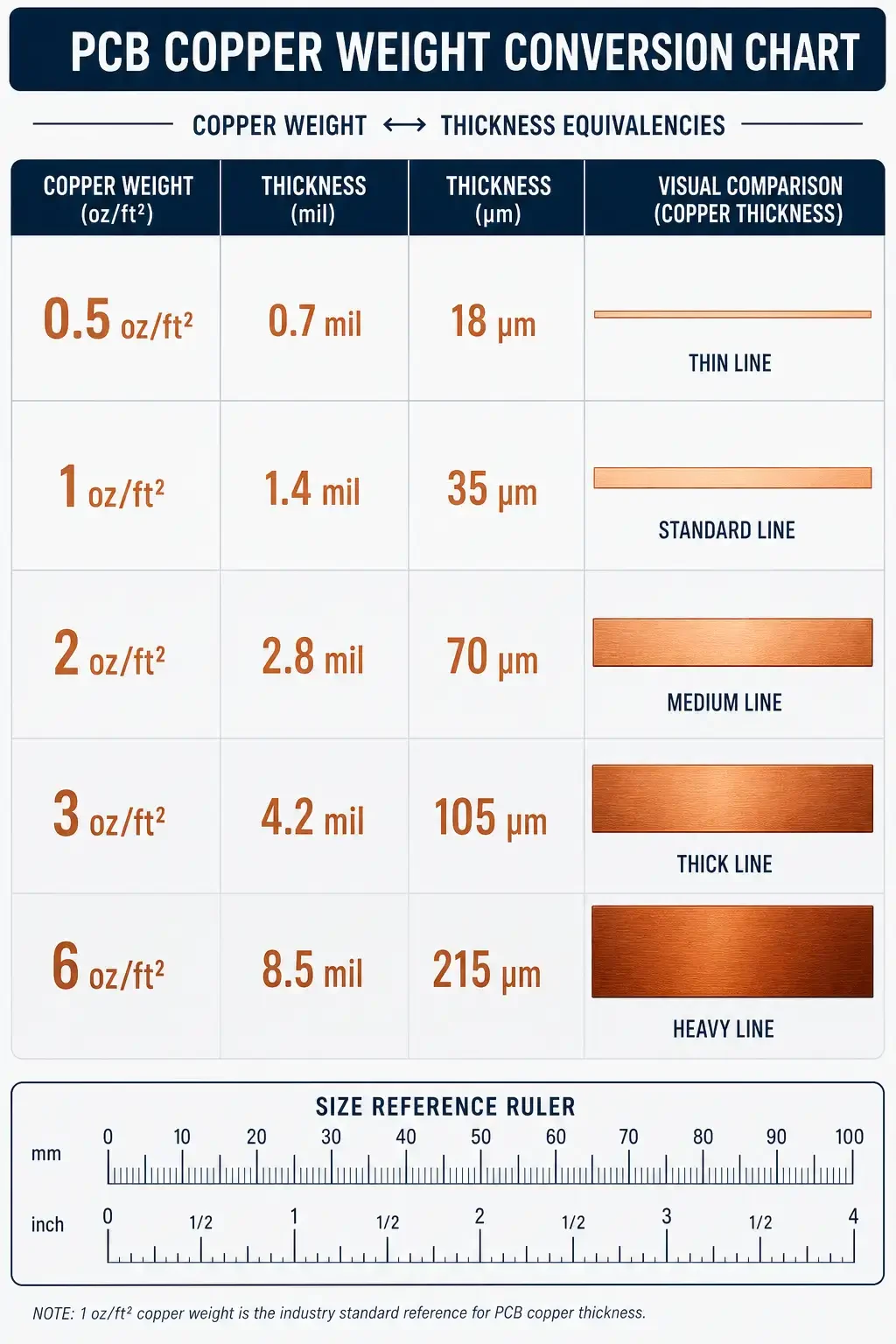
Design software packages typically express copper constraints in mils or millimeters for trace width calculations, while fabrication drawings may specify oz/ft². Engineers must maintain awareness of unit contexts to avoid specification errors that could impact electrical performance or manufacturability. Many PCB design tools include copper weight parameters that automatically calculate current capacity and impedance based on selected thickness values.
Plating processes complicate finished copper weight specification, particularly for multilayer boards. Through-hole plating adds copper to inner layer surfaces and hole walls, potentially increasing outer layer copper thickness. Finished copper weight specifications must indicate whether base foil weight or post-plating thickness is required. Manufacturers adjust etch compensation accordingly, removing additional copper to achieve target finished trace dimensions when plating will add material.
Standard Copper Weights and Applications
Each standard copper weight serves specific application requirements, balancing electrical performance against cost and manufacturing practicality. Understanding typical applications for each weight enables informed selection during schematic and layout phases. Designers should consider future requirements evolution, as board changes to heavier copper later in development incur significant cost and schedule impact.
The 0.5 oz/ft² (18 μm) copper weight represents the lightest standard specification, used primarily for high-density consumer electronics where routing density and cost optimization dominate design priorities. Smartphones, tablets, and wearable devices commonly employ this lightweight copper to achieve compact form factors with maximum routing channels. Signal integrity concerns at high frequencies may favor thin dielectric layers over thin copper, requiring careful stackup optimization.
One-ounce copper (35 μm) serves as the most common standard weight across diverse applications, offering balanced performance for general-purpose circuits. This weight accommodates moderate current requirements while maintaining reasonable trace widths for most routing scenarios. Cost premiums relative to 0.5 oz remain modest, making 1 oz the default specification for many designs without specific high-current or high-frequency requirements.
Two-ounce copper (70 μm) addresses applications requiring enhanced current capacity or improved thermal performance. Automotive electronics, industrial controls, and power supply circuits frequently specify this weight for moderate current traces. Two-ounce copper supports wider current rails while maintaining trace widths manageable for standard PCB fabrication capabilities. However, impedance control becomes more challenging at this thickness, requiring careful modeling.
Three-ounce copper (105 μm) enters the heavy copper category, serving power electronics with substantial current requirements. Motor drives, power converters, and battery management systems commonly employ this weight for main current paths. Fabrication tolerances become looser at this thickness, and fine-pitch routing becomes difficult. Designers should isolate heavy copper regions from high-density signal areas to simplify manufacturing.
Six-ounce copper (215 μm) represents the upper range of standard heavy copper specifications, used for extreme current applications. Bus bars on power distribution boards, high-current power supplies, and welding equipment control boards may specify this weight. Six-ounce copper requires specialized fabrication capabilities including heavy plate-up processes or laminated copper construction. Cost premiums are substantial, and minimum trace widths increase significantly.
Current Carrying Capacity
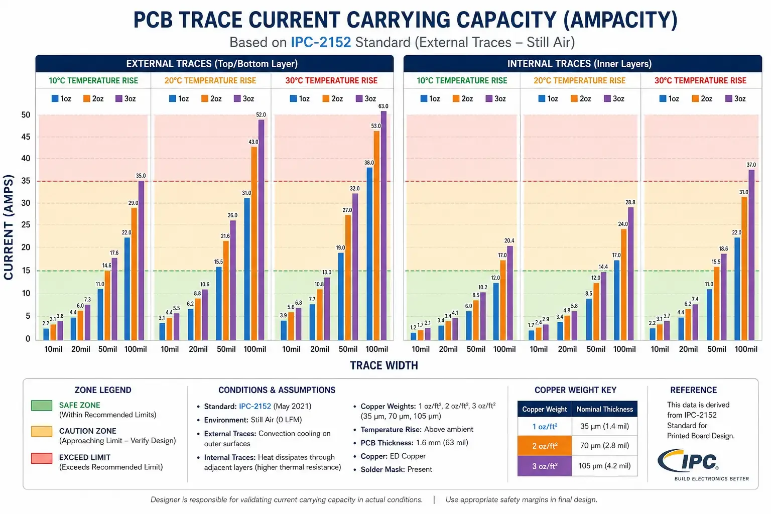
Current carrying capacity, or ampacity, defines the maximum current a conductor can carry without exceeding acceptable temperature rise above ambient conditions. IPC-2152, “Standard for Determining Current-Carrying Capacity in Printed Board Design,” provides the authoritative methodology for calculating PCB conductor ampacity. This standard supersedes earlier IPC-2221 guidance, incorporating improved thermal modeling and empirical testing data.
Ampacity depends on multiple interrelated factors beyond copper weight alone. Trace width determines cross-sectional area available for current flow. Temperature rise allowance defines acceptable thermal budgets. Board material thermal conductivity affects heat dissipation to surrounding environment. Adjacent copper planes, thermal vias, and component proximity influence local temperature rise. Accurate ampacity prediction requires comprehensive analysis considering all relevant parameters.
IPC-2152 presents ampacity data in chart format showing current versus temperature rise for various copper weights and trace widths. Designers select target temperature rise based on application environment and reliability requirements, then determine required trace width for the anticipated current at the specified copper weight. Conservative designs may apply derating factors beyond IPC minimums to provide safety margin.
External traces in free air achieve higher ampacity than internal traces due to convective cooling. IPC-2152 provides separate charts for still air, forced air, and still air with thermal relief conditions. Internal traces with no adjacent copper planes show significantly reduced ampacity compared to external traces. Designers should verify which IPC-2152 conditions apply to specific trace locations within the board stackup.
Track width calculators based on IPC-2152 simplify ampacity calculations for common scenarios. These tools accept inputs including copper weight, trace width, temperature rise, and board configuration (external vs internal, still air vs forced air), then output recommended maximum current. Online calculators and spreadsheet tools incorporate IPC-2152 data for convenient design verification. However, complex thermal environments may require detailed thermal analysis beyond standard calculator capabilities.
Derating factors ensure reliable operation across manufacturing variations and environmental extremes. IPC-2152 recommends applying derating factors of 50-80% to calculated ampacity for conservative designs, accounting for tolerances in copper thickness, trace width, and board thermal properties. Military and aerospace applications apply more stringent derating requirements based on specific reliability standards.
Temperature Rise Considerations
Temperature rise analysis ensures PCB designs operate within acceptable thermal limits throughout product lifecycle. Excessive temperatures accelerate failure mechanisms including solder joint fatigue, dielectric degradation, and conductor electromigration. Understanding temperature rise drivers enables designers to balance electrical performance against thermal constraints.
Ambient temperature significantly impacts allowable temperature rise budgets. A board operating in a 25°C office environment can tolerate 30°C rise, reaching 55°C maximum temperature. The same board in an 85°C industrial enclosure can only tolerate 10°C rise to maintain equivalent absolute temperature margins. Designers must account for worst-case ambient conditions when specifying temperature rise allowances.
Trace geometry determines local heat generation and dissipation balance. Narrow, high-resistance traces generate more heat per unit length for a given current, driving higher local temperatures. Wide traces distribute current across larger cross-sections, reducing resistance and improving heat spreading to adjacent areas. Copper pour areas dramatically improve thermal performance by providing low-resistance paths and large heat-dissipating surfaces.
Thermal vias connect surface traces to internal copper planes or thermal pads, dramatically improving heat dissipation for high-power components. Via thermal conductivity through the board thickness far exceeds air convection on surfaces. Designers should incorporate thermal via arrays beneath power components, MOSFETs, and voltage regulators to direct heat away from sensitive junctions.
Board thickness affects thermal performance through changed geometry and material volume. Thin boards have less thermal mass but also less material for heat spreading. Thick boards provide better heat spreading but may trap heat in internal layers. Stackup optimization balances electrical requirements (impedance control, layer count) against thermal performance, often requiring trade-off analysis for demanding applications.
High-current designs frequently employ specialized thermal management techniques beyond basic copper weight selection. Embedded metal cores, metal-backed substrates, and coin-in-board constructions provide paths for heat removal that exceed standard PCB thermal conductivity. These approaches add cost and complexity but enable power densities impractical with conventional PCB constructions.
Signal Integrity and Impedance Control
Copper weight influences signal integrity through multiple mechanisms affecting high-speed and RF circuit performance. Trace dimensions directly determine characteristic impedance in transmission line structures, while surface roughness and plating affect loss characteristics at high frequencies. Designers of DDR memory interfaces, USB highways, and RF circuits must account for copper weight in their impedance calculations and stackup definitions.
Characteristic impedance (Z0) in controlled impedance designs depends on trace width, dielectric thickness, and dielectric constant per the standard microstrip and stripline equations. Copper thickness appears in the effective width dimension, particularly significant for thin dielectrics where trace height-to-width ratios approach unity. Standard impedance calculators incorporate copper weight parameters to ensure accurate modeling.
Surface roughness effects become significant above several gigahertz. Standard electrodeposited copper foil exhibits roughness of 2-10 microns that disrupts current flow at skin depths approaching similar dimensions. Rough copper increases effective resistance and transmission loss at high frequencies. Low-profile foil options reduce roughness at premium cost, while alternative foil types suit different applications.
Skin effect concentrates current in copper surface regions at high frequencies, reducing effective cross-section and increasing effective resistance. At 10 GHz, skin depth in copper is approximately 0.65 microns, meaning most current flows in the outer copper regions. Surface plating smoothness and uniformity become critical for high-frequency performance, as plating irregularities exceed skin depth thresholds.
Differential pair routing requires careful attention to trace width and spacing for impedance matching. Coupling between pairs depends on geometry including trace width, spacing, and distance to reference planes. Copper weight variation affects trace geometry in ways that influence both differential impedance and common mode characteristics. Designers should use field solvers for critical differential pair optimization.
Inner vs Outer Layer Copper
Multilayer PCB designs require different copper weight considerations for inner and outer layers, driven by distinct processing requirements and performance expectations. Inner layer copper starts as base foil within the board stackup, while outer layers include both base foil and plating additions from through-hole fabrication. This distinction affects both electrical specifications and manufacturing tolerances.
Inner layer copper weight specifications refer to the base foil weight, typically 0.5 to 2 oz/ft² for standard constructions. Heavier inner layer copper complicates registration and imaging for fine-pitch designs, as thicker copper requires longer exposure to achieve complete etching. Inner layer minimum trace widths increase with copper weight, limiting routing density in high-interconnect areas.
Plating processes add copper to outer layers through hole wall electrodeposition. This plating increases outer layer copper thickness beyond base specifications, potentially reaching 1.5 to 2 times base weight after full buildup. Designers should specify finished copper weight requirements for outer layers if thickness control is critical for their application.
Etch factor compensation addresses copper thickness differences between inner and outer layers during fabrication. Inner layer traces are etched from both sides, consuming copper proportional to thickness. Outer layer traces primarily etch from the surface, with less lateral undercut due to plating buildup. Manufacturers adjust artwork scaling accordingly, producing inner and outer layer features at target dimensions despite different processing requirements.
Blind and buried via structures introduce additional complexity for multilayer impedance control. Via stub lengths in sequential lamination affect effective dielectric constants and resonance characteristics. Heavy copper multilayer stacks require careful attention to layer registration and lamination pressure distribution to ensure reliable interconnects.
Differential pair routing across layer transitions (inner to outer) requires careful impedance matching to prevent reflections. Via discontinuities introduce capacitance and inductance perturbations that affect high-speed signals. Ground reference continuity through via antipads, stitching vias, and reference plane continuity management minimize transition effects.
IPC Standards for Copper Thickness
The IPC industry association publishes standards governing PCB materials, design, and acceptability requirements. Several standards address copper thickness specifications and verification methods, providing authoritative reference for designer-manufacturer communication. Understanding these standards enables precise specification and appropriate verification expectations.
IPC-4101, “Specification for Base Materials for Rigid and Multilayer Printed Boards,” classifies laminate materials including copper foil specifications. This standard defines base copper foil requirements including weight tolerances, surface profile specifications, and bonding characteristics. Material datasheets reference IPC-4101 class designations that inform design constraints.
IPC-2221, “Generic Standard on Printed Board Design,” provides comprehensive design guidance including current capacity equations and copper weight selection recommendations. While superseded for ampacity calculations by IPC-2152, IPC-2221 remains relevant for general design practices and family-of-board design guidelines.
IPC-2222, “Sectional Standard for Rigid Organic Printed Boards,” addresses specific design requirements for rigid multilayer boards including layer count recommendations, thickness tolerances, and copper weight specifications. This standard provides the framework for manufacturing capability discussions between designers and fabricators.
IPC-A-600, “Acceptability of Printed Boards,” defines visual and dimensional acceptance criteria including copper thickness verification. This standard specifies measurement methods and acceptance thresholds for finished copper thickness, providing quality reference for incoming inspection and supplier qualification.
Copper thickness verification employs various measurement techniques depending on accuracy requirements and production context. Cross-sectional analysis provides direct physical measurement but destroys the test sample. X-ray fluorescence (XRF) offers non-destructive thickness measurement with acceptable accuracy for production verification. Micro-resistivity instruments infer thickness from electrical measurements, correlating resistance to copper cross-section.
How to Specify Copper Weight in Your Design
Clear copper weight specification ensures manufacturing alignment with design intent and prevents costly misunderstandings. Multiple design deliverables communicate copper requirements including schematic notes, stackup definitions, fabrication drawings, and readme files. Redundant specification reduces misinterpretation risk across diverse manufacturing relationships.
Fabrication drawing specifications should explicitly state copper weight for each layer or layer group, indicating whether base or finished weight applies. Include both oz/ft² and micron equivalents for international clarity. Note any special requirements such as minimum plating thickness for outer layers or plating uniformity tolerances for impedance-controlled designs.
Stackup definitions should incorporate copper weight specifications within layer sequence descriptions. Indicate dielectric materials and thicknesses between signal layers, noting ground and power plane copper weights. Cross-sectional drawings visualize the complete stackup configuration for manufacturing review.
Design files should include copper weight parameters within the design data. Most EDA tools include layer-specific copper weight settings that export with manufacturing data. Gerber files alone do not convey copper weight information; additional files such as IPC-2581 or ODB++ packages or design notes must communicate thickness requirements.
BOM and design documentation should reference copper weight specifications for supply chain alignment. Assembly contractors need copper weight information for stencil design, paste volume calculation, and reflow profile development. Procurement specifications should align with fabrication specifications to ensure consistent board properties across production sources.
Communication with your PCB manufacturer early in the design process identifies available capabilities and cost implications of heavy copper requirements. Manufacturers publish standard capabilities including minimum trace widths, registration tolerances, and layer count limits as functions of copper weight. Early engagement prevents late-stage redesigns when manufacturing limitations surface during production release.
Frequently Asked Questions
How do I convert PCB copper weight from oz/ft² to mils or microns?
One ounce per square foot of copper equals approximately 1.4 mils (35 microns) in thickness. To convert, multiply oz/ft² by 1.4 for mils or by 35 for microns. For example, 2 oz/ft² equals 2.8 mils (2 × 1.4) or 70 microns (2 × 35). This conversion assumes uniform copper distribution over the specified area.
What copper weight is suitable for high-current applications?
High-current applications typically require 2 oz/ft² or heavier copper depending on current magnitude and acceptable temperature rise. For currents exceeding 10A, consider 2-3 oz/ft² with appropriate trace width design. Currents above 30A may require 6 oz/ft² or specialized heavy copper construction. Always verify ampacity using IPC-2152 calculations with appropriate derating factors.
Does copper weight affect PCB manufacturing cost?
Heavier copper increases PCB manufacturing cost due to additional material expense and longer etching times. Costs typically increase 20-50% for 2 oz compared to 1 oz, with steeper increases for 3 oz and heavier. Very heavy copper (>6 oz) may require specialized processing that substantially increases cost. Consider cost implications early in design when specifying copper requirements.
Can I use different copper weights on different layers?
Yes, multilayer PCBs commonly specify different copper weights for inner versus outer layers. Inner layers typically use lighter copper (0.5-1 oz) for fine-pitch routing, while outer layers may use heavier copper (1-2 oz) for current handling and thermal performance. Specify layer-specific weights in your stackup documentation to ensure proper manufacturing implementation.
How does copper weight affect controlled impedance?
Copper weight directly influences trace dimensions in controlled impedance designs, particularly for thin dielectric stacks. Heavier copper increases effective trace width for a given impedance target, affecting routing density and coupling characteristics. Specify copper weight in stackup definitions for impedance-controlled designs, and use field solvers that incorporate thickness parameters.
What minimum trace width can I achieve with different copper weights?
Minimum trace widths increase with copper weight due to etching process limitations. Typical minimum trace widths are approximately 4-5 mils for 1 oz copper, 6-8 mils for 2 oz, and 10-12 mils for 3 oz. Very heavy copper (>6 oz) may require traces of 20 mils or wider. Consult your manufacturer’s capabilities for specific process limits.
References
- IPC-2152, “Standard for Determining Current-Carrying Capacity in Printed Board Design,” IPC International, Inc.
https://www.ipc.org/ - IPC-4101, “Specification for Base Materials for Rigid and Multilayer Printed Boards,” IPC International, Inc.
https://www.ipc.org/ - IPC-2221, “Generic Standard on Printed Board Design,” IPC International, Inc.
https://www.ipc.org/ - IPC-A-600, “Acceptability of Printed Boards,” IPC International, Inc.
https://www.ipc.org/ - “PCB Design Guide for Current-Carrying Capacity,” Macrofab Engineering Blog.
Further Reading
- PCB Surface Finish Comparison: ENIG, HASL, OSP, ENEPIG — Surface finish options affecting solderability and assembly
- Custom PCB Manufacturer — Find suppliers for your specific copper weight requirements
- PCB Quote Requirements — How to specify copper weight in your RFQ documentation
- PCB Stackup Design — Stackup optimization including copper weight considerations
- Controlled Impedance PCB — Impedance control with various copper weights
- Heavy Copper PCB Current Capacity — High-current applications requiring heavy copper
Shanghai Huangte Technology Co., Ltd. | Last updated: 2026-07-24
This article provides general technical guidance for PCB copper weight selection. Specific application requirements may necessitate alternative recommendations. Consult with qualified engineers and your PCB manufacturer for final design decisions.