What Is PCB Prototype Manufacturing?
PCB prototype manufacturing is the specialized branch of PCB production focused on producing a small number of boards—typically 1 to 20 pieces—in the shortest possible time. Unlike mass production, which optimizes for unit cost and throughput, prototype manufacturing prioritizes speed, design validation, and iterative improvement.
A prototype run answers one fundamental question: does the board work as designed? Before that question can be answered, the design must travel through a chain of preparation steps: schematic capture, component selection, PCB layout, design rule verification, and output file generation.
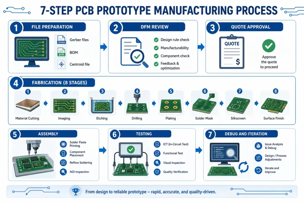
The PCB Prototype Manufacturing Process
Step 1: Design File Preparation
The quality of your output files determines the outcome of your prototype run. Before generating manufacturing files, run a complete Design Rule Check (DRC) in your EDA tool. The DRC catches spacing violations, clearance errors, trace widths below minimums, and drill sizes that exceed manufacturer capability.
A complete prototype PCB manufacturing file package includes:
- Gerber files (RS-274X): One file per copper layer, plus solder mask, silkscreen, and board outline layers.
- Drill files (Excellon format): Contains hole sizes, positions, and plated/non-plated designation for every drill hit.
- Bill of Materials (BOM): A structured list with reference designators, descriptions, manufacturer part numbers (MPN), and quantities.
- Centroid (pick-and-place) file: X/Y coordinates, rotation, and layer designation for each component.
- Assembly drawing: Shows component placement, polarity marks, orientation, and special instructions.
- Stackup and impedance notes: For controlled-impedance designs, include layer stack diagram and target impedance values.
Step 2: Design for Manufacturability (DFM) Review
A DFM review is your manufacturer’s opportunity to catch design errors before fabrication begins. Most prototype manufacturers perform this review as part of their standard process at no additional charge. The review checks:
- Drill checks: Annular ring dimensions (≥0.10-0.125mm), drill aspect ratios (≤8:1), drill-to-copper clearances
- Trace and spacing: Verify trace widths and clearances meet manufacturer minimums (typically 4-5 mil)
- Solder mask: Verify solder mask dams between fine-pitch components
- Silkscreen: Confirm silkscreen text does not overlap pads
- Copper balance: Unbalanced copper can cause warpage during lamination
Step 3: Quote and Approval
A transparent prototype PCB quote breaks down costs into:
- Unit board price: Based on board size, layer count, material, and surface finish
- NRE (Non-Recurring Engineering) fees: One-time setup charges for the first order of a new design:
- CAM engineering and file verification: $30-$100
- SMT stencil fabrication: $50-$200
- Pick-and-place programming: $30-$100
- Flying probe test fixture development: $50-$200
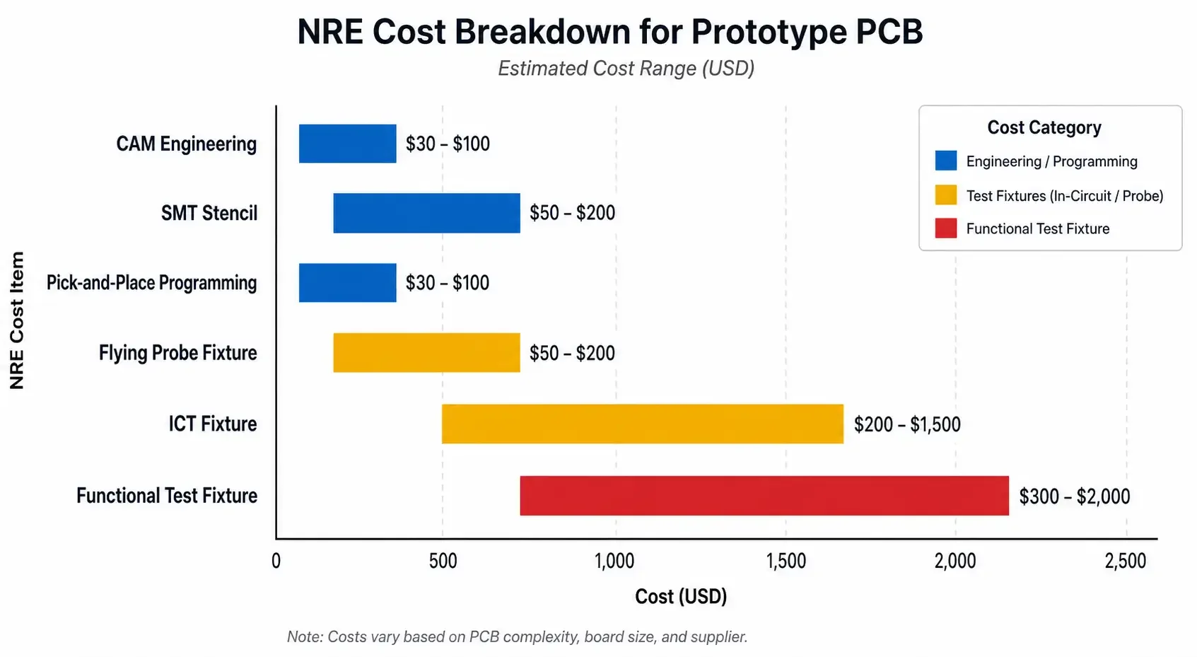
Always request an itemized quote. A lump-sum quote hides the NRE breakdown and makes it impossible to compare offers on equal terms.
Step 4: Fabrication
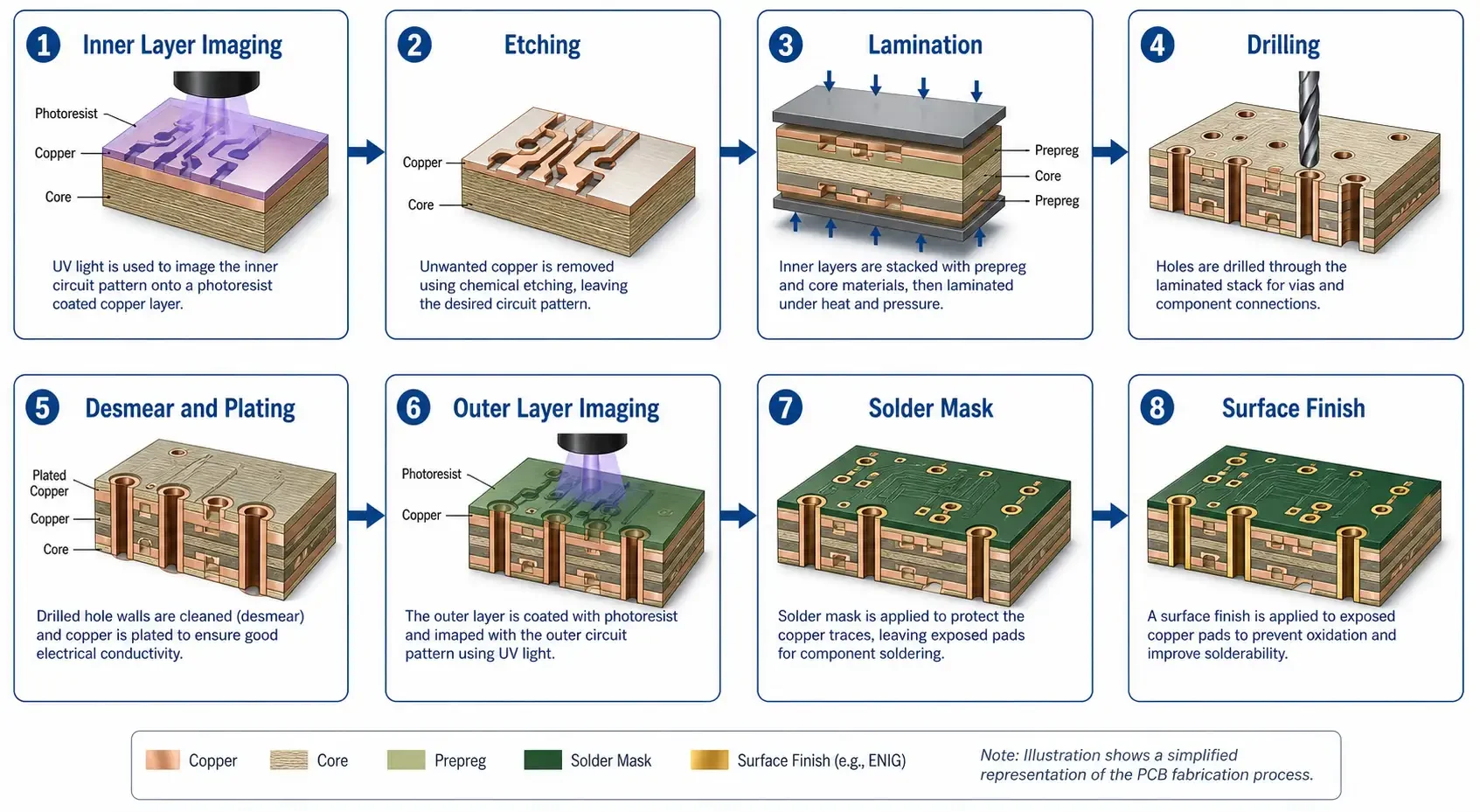
The bare-board fabrication process converts your Gerber files into a physical board. For prototype runs, the core steps are:
- Inner layer imaging and etching: Photoresist is applied, exposed to UV light, and developed. Unwanted copper is etched away.
- Lamination (multilayer boards): Inner layers are aligned, stacked with prepreg, and pressed under heat and pressure.
- Drilling: CNC machines create all through-holes according to the drill file.
- Desmear and copper plating (PTH): Residue is removed and copper is deposited on hole walls.
- Outer layer imaging and pattern plating: Outer layers are imaged and copper is electroplated where needed.
- Etching: Unwanted copper is removed from outer layers.
- Solder mask application: Protective solder mask exposes only pads and holes.
- Surface finish: ENIG, HASL, OSP, or Immersion Silver protects exposed copper pads.
- Silkscreen/legend: Reference designators and markings are printed.
- Routing and singulation: Panel is routed or scored to separate individual boards.
- Electrical test: 100% of boards undergo electrical test to verify all nets are correctly connected.
Step 5: Assembly (Optional)
If you ordered turnkey prototype assembly, components are placed and soldered after the bare board passes electrical test:
- Solder paste printing: A stencil applies solder paste to the pads.
- Component placement: Automated pick-and-place machines position components.
- Reflow soldering: The board passes through a reflow oven with controlled heating.
- Through-hole insertion: Through-hole components are inserted and soldered.
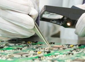
- Inspection: AOI checks for placement errors; X-ray verifies hidden joints under BGA and QFN.
Step 6: Testing and Validation
Testing transforms a fabricated board into a validated prototype:
- Flying probe test: Checks all nets for opens, shorts, and isolation faults. Non-contact, no fixture required.
- Automated Optical Inspection (AOI): Detects component placement errors and visible defects.
- X-ray inspection: Inspects hidden solder joints under BGA and QFN packages.
- Solder Paste Inspection (SPI): Verifies solder paste volume before reflow.
- Functional Circuit Test (FCT): Applies power and test signals to verify board function.
Step 7: Debug, Iteration, and Production Transition
The first powered prototype rarely passes every test. This is expected. Debug involves identifying failures, fixing the schematic or layout, generating new files, and submitting for another prototype run.
Each iteration should close specific open items rather than reopening the entire design. The goal of prototype manufacturing is to converge on a validated design that transitions smoothly to production.
Typical Timeline and Lead Times
| Board Type | Layer Count | Standard Lead Time | Quick-Turn Lead Time |
|---|---|---|---|
| Standard rigid (FR-4) | 1-2 layers | 5-10 business days | 24-48 hours |
| Standard rigid (FR-4) | 4-6 layers | 10-15 business days | 2-3 business days |
| Standard rigid (FR-4) | 8-12 layers | 15-20 business days | 3-5 business days |
| HDI / Advanced | 4-8 layers | 15-25 business days | 5-7 business days |
| Flex / Rigid-Flex | 2-4 layers | 15-25 business days | 5-7 business days |
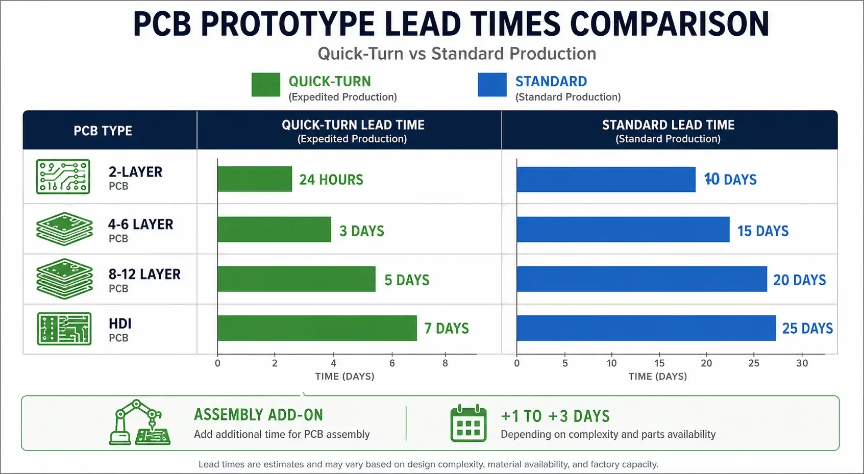
Lead times are measured from Gerber approval and payment confirmation—not from order submission. File review and DFM feedback add 4-24 hours before fabrication begins. Assembly adds 1-3 days to the total timeline.
Cost Factors for PCB Prototypes
Prototype PCB costs appear disproportionately high compared to production because setup costs (NRE) are spread across a small number of boards. On a 10-piece prototype order with $200 in total NRE, the setup cost adds $20 per board. On a 1,000-piece production order, the same $200 NRE adds only $0.20 per board.
NRE impact by quantity:
| Order Quantity | Typical NRE per Board | Notes |
|---|---|---|
| 1-10 pieces | $50-$100 | Full NRE spread |
| 100 pieces | $5-$10 | NRE amortized |
| 1,000 pieces | $0.50-$1.00 | Negligible NRE impact |
Quick-turn premium: Expedited fabrication adds 30-200% to standard pricing. Budget for this premium if your project timeline requires it.
Common Mistakes to Avoid
- Skipping the DRC before generating files. Run the DRC in your EDA tool and fix every error before exporting.
- Not using manufacturer part numbers in the BOM. Use exact MPNs to accelerate component sourcing.
- Omitting the centroid file for assembly. Without it, the manufacturer must derive placement data from the layout.
- Ignoring the DFM report. Review it promptly and address critical items before fabrication begins.
- Selecting the wrong surface finish. Choose ENIG for fine-pitch components and flatness requirements.
- Forgetting test points. Designing in accessible test points reduces debug time dramatically.
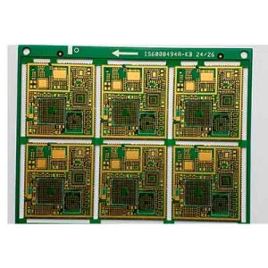
- Not panelizing for small runs. A 2×2 or 2×4 panel maximizes usable boards.
Frequently Asked Questions
Q1: What files do I need for prototype PCB manufacturing?
A complete prototype file package includes:
- Gerber files (RS-274X) for all copper, solder mask, silkscreen, and board outline layers
- Drill files (Excellon format) with plated/non-plated designations
- Bill of Materials (BOM) with manufacturer part numbers and quantities
- Centroid/pick-and-place file with X/Y coordinates and rotation for each component
- Assembly drawing with placement instructions and polarity markings
- Stackup and impedance notes for controlled-impedance designs
Q2: How long does prototype PCB manufacturing take?
Standard prototype lead times range from 5 to 20 business days depending on complexity. Quick-turn options: 2-layer boards 24-48 hours, 4-6 layers 2-3 days, 8-12 layers 3-5 days. These timelines start from Gerber approval—not order submission.
Q3: What is the minimum order quantity for prototypes?
Most prototype manufacturers accept 1 to 5 pieces for prototype runs. Some quick-turn services offer single-board fabrication.
Q4: Can I get assembly with my prototype?
Yes. Turnkey prototype assembly includes component procurement, SMT placement, inspection, and testing. Lead time typically adds 1-3 business days after bare board fabrication.
Q5: What happens if my prototype fails testing?
Testing failures are expected during prototyping. For bare board failures, contact the manufacturer for investigation and potential replacement. For functional failures, fix the design and submit a new prototype run.
References
- PCBSync. “PCB Manufacturing Process: Complete 16-Step Guide [2026].” https://pcbsync.com/pcb-manufacturing-process/
- Zeus Design. “Circuit Board Design: How the PCB Process Works in 2026.” https://zeusdesign.com.au/circuit-board-design-how-the-pcb-process-works-in-2026
- Tech Tempted. “PCB Prototyping: From Design to First Boards.” https://techtempted.com/pcb-prototyping-from-design-to-first-boards/
- RapidDirect. “PCB Prototype Manufacturing: Step-by-Step from Design to Test.” https://www.rapiddirect.com/blog/pcb-prototype-manufacturing-guide/
- Queen EMS. “What Does NRE Mean on a PCB Quote?” https://www.queenems.com/blog/what-does-nre-mean-how-to-reduce-pcb-setup-tooling-costs/
- Bittele Electronics. “Non-Recurring Engineering (NRE) and Tooling Costs.” https://www.7pcb.com/blog/nre-tooling-costs
- PCBAndAssembly. “Custom PCB Board Price: Complete Guide to PCB Manufacturing Costs.” https://pcbandassembly.com/blog/custom-pcb-board-price-complete-guide-to-pcb-manufacturing-costs/
- PCBSync. “PCB DFM Checklist: 25 Critical Items.” https://pcbsync.com/dfm-checklist-pcb/
Further Reading
- PCB Manufacturing & Assembly — Overview of PCB manufacturing and assembly services, covering the complete workflow from design files to finished boards.
- PCB Fabrication Process Explained — Detailed breakdown of the PCB fabrication process stages, from material preparation through electrical testing.
- One-Stop PCB PCBA Service — Explanation of turnkey services that cover PCB fabrication, component sourcing, assembly, and testing under one roof.
- How to Choose PCBA Manufacturer — Practical guide on evaluating PCB assembly manufacturers based on capabilities, quality standards, and service scope.
Shanghai Huangte Technology Co., Ltd. | Last updated: 2026-07-18
This article is for informational purposes and does not constitute professional engineering or legal advice. Specific PCB requirements should be verified with qualified manufacturers and reviewed by a licensed professional engineer.