Why a Complete RFQ Matters
An RFQ package serves two purposes: it allows the manufacturer to assess whether they can produce your board, and it provides the information needed to generate an accurate price. Incomplete packages create uncertainty that manufacturers resolve through one of two responses: they decline to quote until they receive complete information, or they quote based on assumptions that may not match your actual requirements.
When a manufacturer assumes your board is 1.6mm thick, ENIG surface finish, and IPC Class 2, and your actual requirements are 2.0mm, HASL, and Class 3, the quote will be significantly off. Resolving this mismatch after you have committed to a purchase order wastes time and may require order cancellation and re-quoting.
Beyond pricing accuracy, complete specifications allow the manufacturer to identify potential manufacturing challenges early. A board with tight impedance tolerance, complex stack-up, or non-standard material benefits from DFM feedback before you commit to production. This feedback is only possible when the manufacturer has complete information.
Essential Gerber Files
Gerber files are the universal language of PCB fabrication. The Gerber format, originally developed by Gerber Systems Corporation and now maintained by Ucamco, represents the de facto standard for PCB manufacturing data transfer. All PCB design tools export Gerber files, and all PCB fabrication software processes them.
Required Layer Files
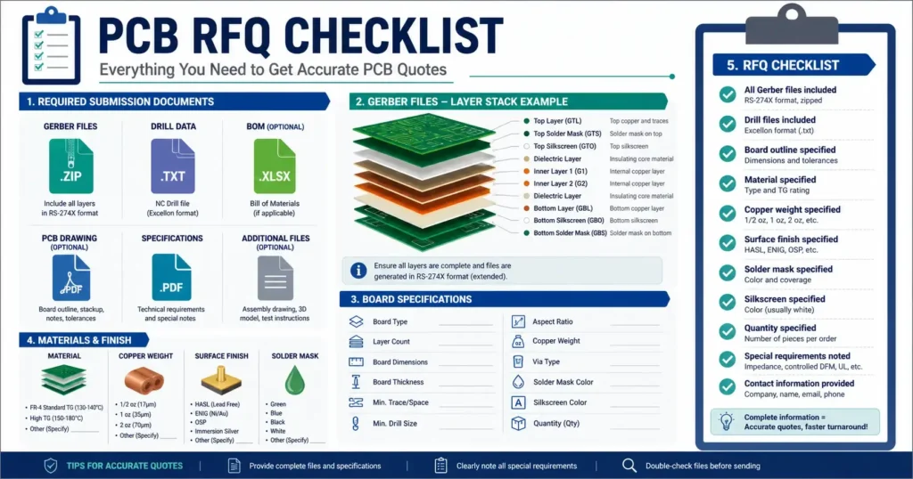
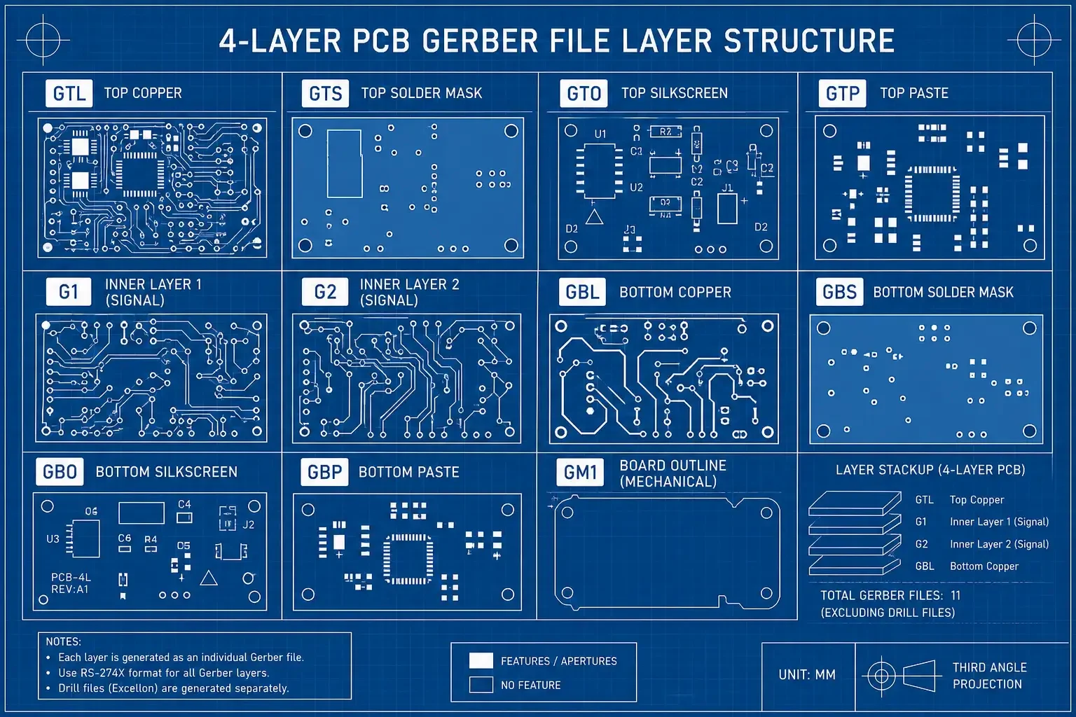
A complete Gerber package for PCB fabrication includes:
- Copper layers: One file for each conductive layer. Standard naming uses layer codes such as GTL (Top Copper), GBL (Bottom Copper), G1 through Gn for inner layers. Some EDA tools use descriptive names or sequential numbering—consistency within the package matters more than the specific naming convention.
- Solder mask layers: One file for each solder mask layer. Standard naming uses Suffix notation: GTS (Top Solder Mask), GBS (Bottom Solder Mask), G1S through GnS for inner layer mask (if applicable). Solder mask files define the areas where solder mask should NOT be applied—pads, holes, and fiducials remain exposed.
- Silkscreen/legend layers: One file for each legend layer. Standard naming uses GTO (Top Overlay), GBO (Bottom Overlay). Silkscreen files define text, logos, component outlines, and other markings printed on the board surface.
- Paste layers (for SMT assembly): GTP (Top Paste), GBP (Bottom Paste). Paste layers define stencil openings for solder paste application during assembly. Include these if you are ordering turnkey assembly services.
- Board outline: A file defining the board shape, typically named GM1 or similar. The outline must be a closed shape without gaps or overlaps. Panelization for production should be specified separately.
Gerber Format Versions
RS-274X (Extended Gerber) is the current standard format for Gerber files. It is the default output from virtually all modern EDA tools. RS-274D (Basic Gerber) is obsolete and should not be used. Gerber X2 adds attributes to the format that provide metadata about pads, vias, and net names. While Gerber X2 is increasingly supported, confirm compatibility with your manufacturer.
File Quality Verification
Before submitting Gerber files, verify the following:
- All layers are present and accounted for
- Board outline exists and forms a closed shape
- Drill file references match the copper layer count
- Solder mask openings correspond to copper pads
- No negative features in copper layers (unless specifically intended)
Drill Files and Plated/Non-Plated Requirements
Drill files define the location, size, and type of every hole in the board. The Excellon format is the standard for PCB drill data. Excellon files contain drill hit coordinates and tool assignments that the manufacturer’s CNC drilling equipment uses to produce holes.
Plated Through-Hole (PTH) vs Non-Plated Through-Hole (NPTH)
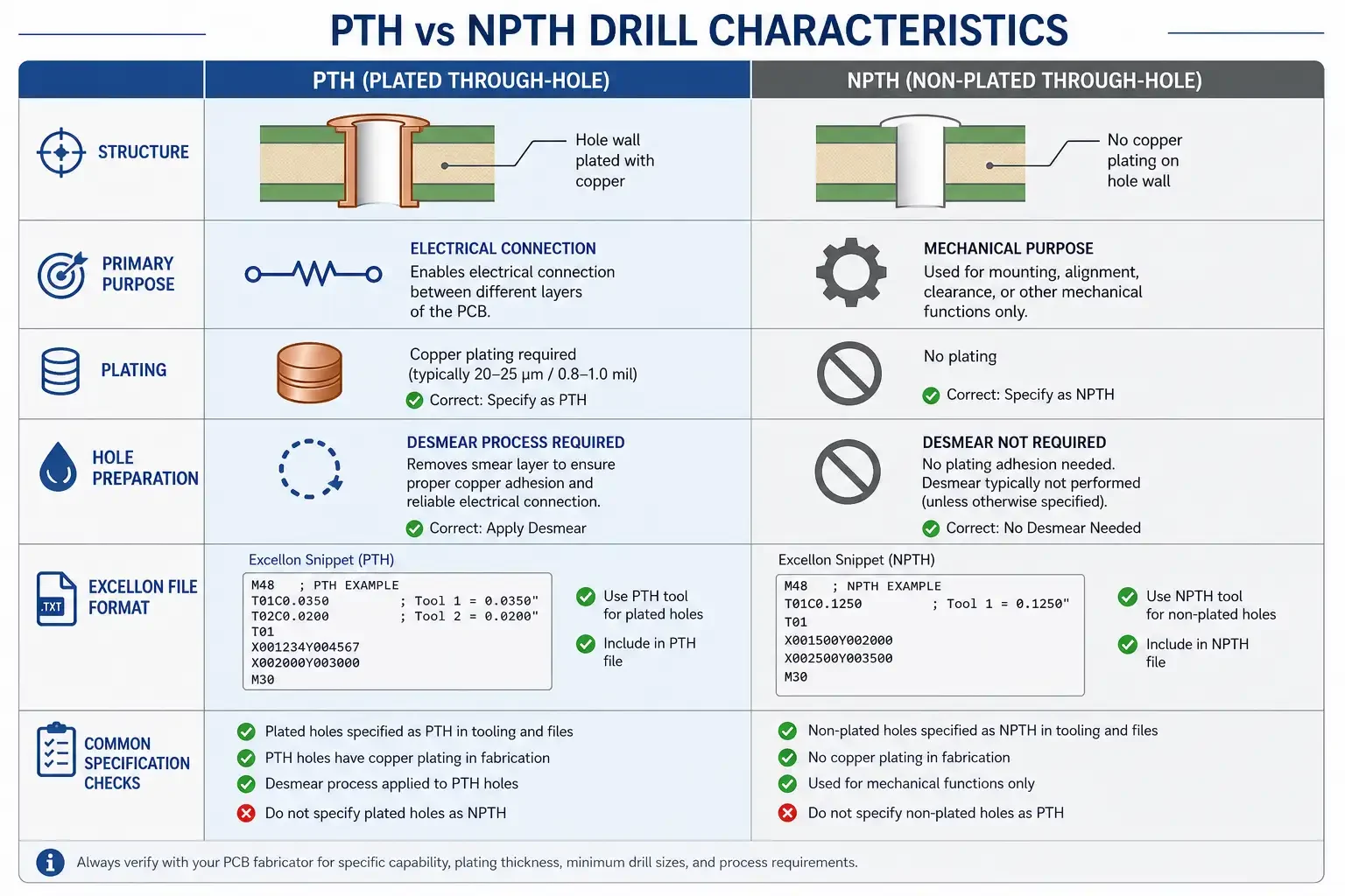
The most critical distinction in drill files is plated versus non-plated holes. Plated through-holes (PTH) have copper plating on the hole wall that electrically connects multiple layers. Non-plated through-holes (NPTH) have no plating—they are simply holes through the board for mechanical purposes such as mounting screws, standoffs, or ventilation.
Failing to distinguish PTH from NPTH causes manufacturing errors. Plated holes require desmear treatment and electroless copper seed layer before electroplating—the manufacturer must know which holes require this process. Confusion between PTH and NPTH can result in incorrect plating, assembly problems, or board rejection.
The Excellon format uses tool definitions to distinguish PTH from NPTH. Ensure your EDA tool’s drill file output correctly categorizes holes. Common convention uses “Plated” or “PTH” in the tool definition comment, or groups PTH and NPTH into separate files.
Drill File Requirements
Verify your drill file includes correct hole sizes matching the design, correct coordinates in the board’s design origin system, plated/non-plated designation for each tool, and any slot or routed slot definitions (not all EDA tools output these correctly).
Board Specifications
Board specifications define the physical and material requirements that Gerber and drill files alone do not specify.
Material Selection
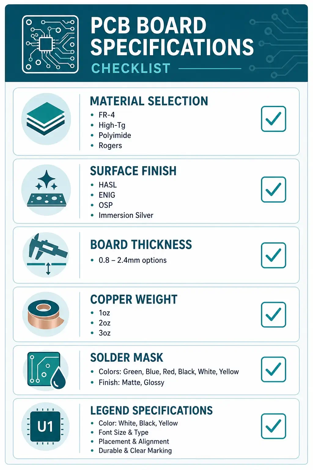
The base material affects electrical performance, thermal behavior, mechanical strength, and cost. Standard options include:
- FR-4 (Standard Tg): General-purpose epoxy-glass laminate. Suitable for most commercial applications. Tg (glass transition temperature) of approximately 130°C.
- FR-4 (High Tg): Enhanced thermal performance with Tg of 150°C or higher. Required for lead-free assembly processes that expose boards to higher reflow temperatures. Recommended for thick boards and boards with significant thermal mass.
- FR-4 (Mid-Tg): Tg of approximately 140°C. A compromise between standard and high-Tg for applications that need some thermal margin without the cost premium of high-Tg.
- Polyimide: High-temperature material for applications requiring extreme thermal resistance. Used in aerospace, defense, and high-reliability industrial applications. Higher cost and longer lead times than FR-4.
- Rogers High-Frequency Laminates: Specialized materials for RF and microwave applications. Offer controlled dielectric constant and low loss tangent at high frequencies. Significant cost premium and typically longer lead times.
Surface Finish
Surface finish protects exposed copper pads from oxidation and provides solderability for assembly. The finish selection affects shelf life, solderability, flatness, and cost.
- HASL (Hot Air Solder Leveling): Traditional finish using solder alloy applied by hot air knife. Cost-effective and provides good solderability. May not be suitable for fine-pitch components due to uneven surface from the leveling process.
- Lead-Free HASL: RoHS-compliant alternative to traditional HASL. Similar characteristics and limitations.
- ENIG (Electroless Nickel Immersion Gold): Two-layer finish with nickel barrier and gold surface. Provides flat surface ideal for fine-pitch components and BGA packages. Good shelf life. Higher cost than HASL.
- OSP (Organic Solderability Preservative): Chemical coating that protects copper. Low cost and flat surface. Limited shelf life (typically 3-6 months).
- Immersion Silver: Silver surface with good solderability and flatness. Moderate shelf life. An alternative to ENIG for cost-sensitive applications.
Board Thickness
Standard thicknesses include 0.8mm, 1.0mm, 1.2mm, 1.6mm, 2.0mm, and 2.4mm. The most common thickness is 1.6mm (approximately 0.063″). Specify your required thickness and tolerance if non-standard.
Copper Weight
Base copper weight (before plating) and finished copper weight (after plating) differ. Standard options include 1oz (35μm), 2oz (70μm), and 3oz (105μm) copper. Finished copper weight is typically 1.5-2 times base copper due to plating buildup. Specify base copper weight if your design requires specific current capacity.
Solder Mask and Legend
Specify solder mask color (green, red, blue, black, white, yellow, etc.) and finish (matte or glossy). Specify legend/silkscreen color (typically white on green mask, white or black on other colors). Indicate any specific silkscreen requirements or exclusions.
Special Requirements
Many applications require specifications beyond the standard fabrication package.
Controlled Impedance
If your board includes impedance-controlled traces, specify target impedance values and tolerances, the reference planes for each controlled impedance net, and which layers contain controlled impedance traces. The manufacturer needs this information to verify stack-up and produce impedance test coupons.
IPC Class
Indicate the required IPC class level:
- Class 1 (General): Consumer products where functional performance is primary concern
- Class 2 (Dedicated Service): Commercial and industrial equipment
- Class 3 (High Performance): Aerospace, medical, military, automotive safety
Higher class levels require more inspection, tighter tolerances, and additional documentation—all of which affect cost.
UL Rating
Specify the required UL flame rating, typically UL 94 V-0 for commercial products. Verify the manufacturer holds UL authorization for your specific board construction.
Test Requirements
Indicate required electrical testing:
- Flying probe test (non-contact, no fixture required)
- Fixture test (bed-of-nails fixture for production testing)
- Impedance test (TDR measurement of controlled impedance traces)
Special Testing and Documentation
For Class 3 or high-reliability applications, additional requirements may include microsection/cross-section analysis, certificate of conformance (C of C), material certificates and traceability, and first article inspection (FAI) report.
Optional but Recommended
Several additional items improve quote accuracy and prevent downstream issues.
Panelization
Specify whether you require panelization for production quantities. Panelization involves arranging multiple boards on a fabrication panel with tooling holes, breakaway tabs, or V-scoring. If not specified, the manufacturer will panelize according to their standard practices.
Quantity Breaks
Request pricing for multiple quantity tiers (e.g., 10, 50, 100, 500 pieces) to understand the cost curve. This information is valuable for inventory and production planning decisions.
DFM Report
Request a DFM (Design for Manufacturability) report as part of the fabrication package. The DFM review identifies potential manufacturing issues before fabrication begins, giving you the opportunity to resolve problems without delaying production.
Frequently Asked Questions
Q1: What Gerber files are required for a PCB quote?
At minimum, provide copper layers for all conductive layers, solder mask layers for top and bottom, silkscreen/legend layers for top and bottom, and a board outline file. If ordering assembly, include paste layers for SMT pads. Verify all layers export without errors and that the board outline forms a closed shape.
Q2: What is the difference between PTH and NPTH drill files?
PTH (Plated Through-Hole) holes have copper plating on the hole wall that electrically connects layers. NPTH (Non-Plated Through-Hole) holes have no plating and are purely mechanical (mounting holes, ventilation). Your EDA tool must correctly designate each hole type in the drill file. Mixing up PTH and NPTH causes manufacturing errors that may require board respin.
Q3: Do I need to include impedance specifications in the RFQ?
Yes, if your board includes impedance-controlled traces. Specify target impedance values (e.g., 50Ω single-ended, 100Ω differential), tolerance (typically ±10% or ±5%), and which layers contain controlled impedance traces. The manufacturer needs this information to verify the stack-up design and produce impedance test coupons.
Q4: What surface finish should I specify?
The appropriate finish depends on your assembly requirements. HASL is cost-effective for through-hole and larger pitch components. ENIG is preferred for BGA, fine-pitch QFP, and applications requiring flat surface and extended shelf life. OSP is a low-cost option for boards that will be assembled quickly. Consult your assembly contractor if you are unsure—they often have preferences based on their assembly process.
Q5: How detailed should my BOM be?
A complete BOM includes reference designator, quantity, description, manufacturer part number (MPN), and any alternate parts. MPNs are essential for turnkey assembly to source exact components. Include lifecycle status (active, NRND, obsolete) and any special handling requirements. Incomplete BOMs delay assembly quoting and risk component substitution without your knowledge.
References
- Ucamco. “Gerber Format Specification.”
https://www.ucamco.com/en/gerber - IPC-2221: Generic Standard on Printed Board Design. IPC.
https://www.ipc.org/ - IPC-A-600: Acceptability of Printed Boards. IPC.
https://www.ipc.org/ - IPC-6012: Qualification and Performance Specification for Rigid Printed Boards. IPC.
https://www.ipc.org/ - SMTA. “Best Practices for Electronics Assembly.”
https://www.smta.org/
Further Reading
- Custom PCB Manufacturer: How to Choose the Right Partner for Prototype and Production — Finding a qualified PCB supplier
- PCB Prototype Manufacturing: From Design Files to a Testable Board — File preparation for prototype orders
- Quick-Turn PCB Prototypes: What Can Be Fast-Tracked and What Cannot — Expedited quote considerations
- Low-Volume PCB Manufacturing: When a Pilot Run Is Better Than Mass Production — Low-volume RFQ planning
- Selecting a Multilayer PCB Manufacturer: Stack-Up, Registration and Reliability — Multilayer PCB manufacturing guide
Shanghai Huangte Technology Co., Ltd. | Last updated: 2026-07-20
This article is for informational purposes and does not constitute professional engineering or legal advice. Specific PCB requirements should be verified with qualified manufacturers and reviewed by a licensed professional engineer.