Why 4-Layer PCBs Are Popular
The 4-layer PCB sits in a sweet spot that few other configurations match. Two-layer boards are cheaper but cannot reliably host controlled impedance traces, have minimal shielding, and force designers to make tough routing compromises. Six-layer and higher boards provide more routing channels and better signal integrity but add cost, lead time, and stack-up complexity that few designs actually need.
A 4-layer board resolves these constraints efficiently. The two inner planes provide dedicated reference and power distribution, the two outer layers host signal routing, and the manufacturing process is well-established at virtually every PCB fabrication house. For designers, this means shorter lead times, predictable impedance behavior, and the freedom to use standard FR-4 materials for most applications.
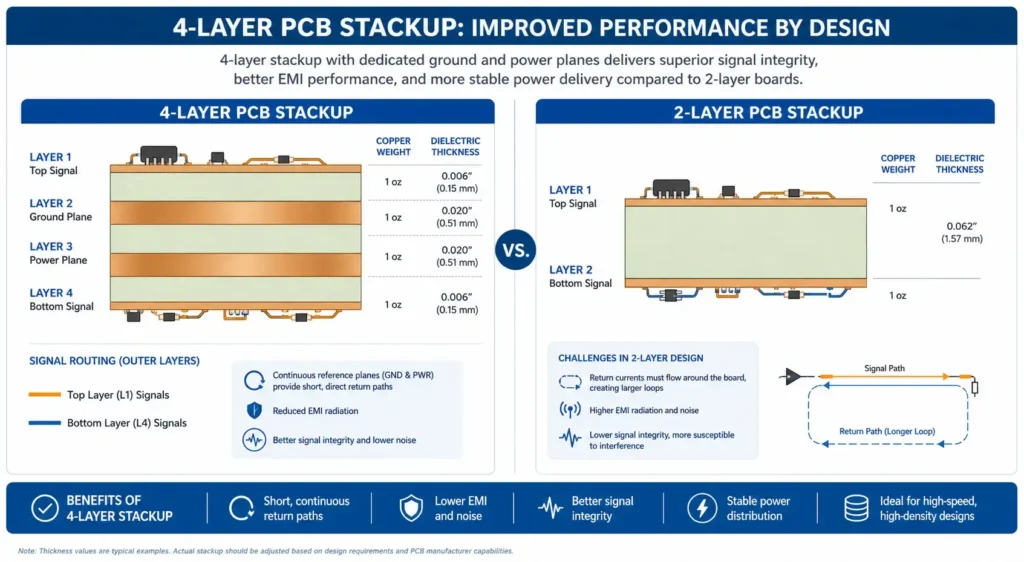
The performance gains over 2-layer designs are substantial. With a continuous ground plane adjacent to the top signal layer, return currents have a clear low-impedance path. The power plane reduces voltage drop and provides additional shielding. Crosstalk drops because the planes absorb field energy, and EMI emissions fall because return currents stay contained.
Cost-wise, a 4-layer board typically runs 30–60% more than a 2-layer board of the same size while supporting more advanced interfaces. Compared to a 6-layer board, a 4-layer board is usually 20–40% cheaper and delivers most of the signal integrity benefits that 6-layer designs are typically chosen for.
Standard 4-Layer Stack-Up Configurations
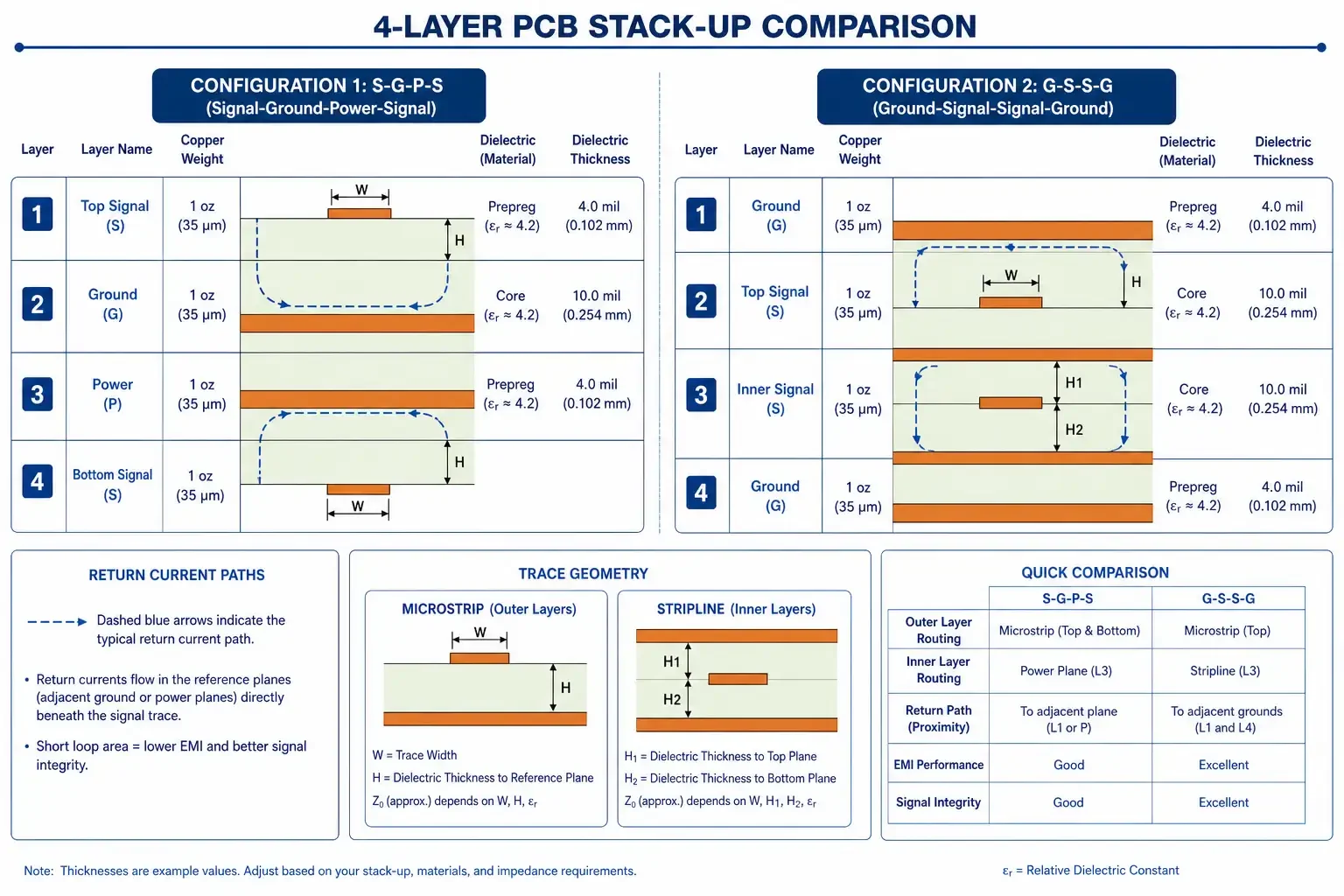
There are two widely used 4-layer arrangements. The choice depends on which signals are most critical and whether inner stripline routing is needed.
Configuration A: Signal–Ground–Power–Signal (S-G-P-S)
The standard 4-layer PCB stackup places signal layers on the outside and planes on the inside. This is the default choice for the vast majority of 4-layer designs.
| Layer | Type | Function |
|---|---|---|
| 1 | Signal | Top components, critical routing, microstrip with reference to layer 2 |
| 2 | Ground | Continuous ground plane, return path for layer 1 signals |
| 3 | Power | Power distribution, partial shielding, optional split for multiple rails |
| 4 | Signal | Bottom components, less critical routing, microstrip with reference to layer 3 |
This arrangement places every outer signal trace within a controlled distance of a reference plane. Top signals reference the ground plane; bottom signals reference the power plane. The two planes also create a distributed decoupling capacitance between them, which supplements discrete decoupling capacitors at high frequencies.
Configuration B: Ground–Signal–Signal–Ground (G-S-S-G)
When inner-layer stripline routing is required—such as for sensitive signals that need shielding on both sides—a G-S-S-G arrangement is used. Both signal layers sit between ground planes, and power distribution is handled by routing on inner signal layers or by adding power islands.
| Layer | Type | Function |
|---|---|---|
| 1 | Ground | Reference for layer 2, outer ground pour for shielding |
| 2 | Signal | Inner stripline with references to layers 1 and 3 |
| 3 | Signal | Inner stripline with references to layers 2 and 4 |
| 4 | Ground | Reference for layer 3, outer ground pour |
This configuration is less common because it complicates power distribution. Power rails must be routed as traces or as power islands on the signal layers, which uses routing space. However, for RF sections, analog blocks, or designs that need maximum shielding on inner signal traces, G-S-S-G is the right choice.
Configuration Comparison
| Configuration | Top Layer | Bottom Layer | Best For | Trade-Offs |
|---|---|---|---|---|
| S-G-P-S | Signal | Signal | General digital, mixed-signal, USB, HDMI, DDR3 | Bottom signals reference power plane, not ideal for high-speed |
| G-S-S-G | Ground | Ground | RF, sensitive analog, inner stripline needs | Power distribution is harder, less routing space |
Layer Arrangement Principles
The principles that guide 4-layer stack-up design are simpler than for higher layer counts, but they are not optional. Each rule addresses a specific signal integrity or manufacturability issue.
Adjacent Reference Planes
Every signal layer in a 4-layer board should have a reference plane directly adjacent. In the standard S-G-P-S arrangement, layer 1 references layer 2 (ground) and layer 4 references layer 3 (power). Signals that lose their reference—for example, a trace routed over a power plane split—experience impedance discontinuities, increased crosstalk, and EMI problems. Avoid routing across plane splits on layer 3.
Ground Plane Priority
Place the ground plane on layer 2 (directly below the top signal layer) rather than on layer 3. This minimizes return current loop area for the most heavily routed layer and ensures the best signal integrity for top-side high-speed signals. The reason is that high-speed components and dense routing typically live on the top side.
Power and Ground Proximity
Keep the ground and power planes physically close to each other. The thin dielectric between layers 2 and 3 forms a distributed capacitor that supplements decoupling. A 0.5 oz copper ground/power pair with 8 mil dielectric provides approximately 40 pF per square inch of overlap area. This capacitance is effective at frequencies above 100 MHz, where discrete capacitors lose effectiveness due to ESL.
Symmetry for Manufacturability
A symmetric stack-up (identical construction above and below the board center) reduces warpage during lamination and reflow. For a 4-layer board, this means equal dielectric thickness and copper weight on layers 1/4 and on layers 2/3. Asymmetric stack-ups are acceptable for hand-assembled or through-hole designs but should be minimized when surface-mount components will be assembled.
Ground and Power Plane Design
The two internal planes are the heart of a 4-layer PCB stack-up. How they are designed has a greater effect on electrical performance than almost any other stack-up decision.
Continuous Ground Plane
The ground plane should be as continuous as possible. Avoid cutting slots in the ground plane unless absolutely necessary. Each slot forces return currents to detour around it, increasing loop area and EMI. If signals must cross a plane discontinuity, add a stitching capacitor or bridge trace to maintain return path continuity.
Power Plane Strategy
For designs with a single supply voltage, a solid power plane on layer 3 is ideal. For multiple supply voltages (e.g., 3.3 V, 1.8 V, 1.2 V), the plane can be split, but each split must be managed to avoid signal integrity problems. Place components using the same supply near each other to minimize trace length across splits.
Decoupling Capacitor Placement
Place decoupling capacitors as close as possible to the power pins of each IC. Use a combination of bulk (1 µF+), mid-frequency (0.1 µF), and high-frequency (10 nF and below) capacitors. The plane-to-plane capacitance supplements discrete capacitors above 100 MHz.
Return Current Path
High-frequency return currents follow the path of least impedance, which is directly beneath the signal trace on the adjacent reference plane. Never route a high-speed signal across a plane split without a return path bridge. Crossing a ground-to-power split forces the return current through decoupling capacitors or stitching vias, which adds inductance and noise.
Controlled Impedance in 4-Layer Boards
Most 4-layer boards that target any modern interface require controlled impedance. The good news is that the standard S-G-P-S stack-up supports microstrip on both outer layers, which is the easiest geometry to model and manufacture.
Top Microstrip
Traces on layer 1 reference the ground plane on layer 2. Impedance is controlled by trace width, copper thickness, and the dielectric thickness between layer 1 and layer 2. For 50 Ω single-ended impedance on FR-4 (Dk ≈ 4.3), typical dimensions are 8–10 mil trace width with 6–8 mil dielectric to ground for 1 oz copper.
Bottom Microstrip
Traces on layer 4 reference the power plane on layer 3. The geometry is similar to top microstrip, but designers should be aware that the reference is the power plane. If the power plane is split for multiple rails, bottom-side signals routed over different splits may experience different reference conditions.
Inner Stripline
Standard S-G-P-S does not support stripline because both internal layers are planes. For inner stripline, use the G-S-S-G arrangement. Stripline offers better shielding than microstrip and is preferred for sensitive signals.
Differential Pairs
USB, HDMI, and DDR data signals use differential pairs. The differential impedance target is typically 90 Ω (USB), 100 Ω (Ethernet, many LVDS interfaces), or 85 Ω (some PCIe variants). Trace width, spacing, and distance to the reference plane must be modeled together. Use a field solver for accuracy, especially for tight tolerance requirements.
Impedance Modeling Workflow
- Identify the stack-up geometry: dielectric thickness between each layer, copper weight, and material Dk.
- Define target impedance for each controlled net: 50 Ω single-ended, 90/100 Ω differential, or other.
- Use a field solver (Polar Instruments Si9000, Saturn PCB Toolkit, or similar) to calculate required trace width and spacing.
- Verify calculated widths and spacings are within your manufacturer’s manufacturing capability.
- Document the final impedance values in the stack-up drawing and the fabrication notes.
Always confirm the impedance calculation with your manufacturer. Dielectric constant values vary between material lots, and manufacturers calibrate their models to specific suppliers. The numbers your field solver gives are a starting point; the numbers your manufacturer provides are the production target.
Material Selection for 4-Layer Boards
Material selection for 4-layer boards is generally simpler than for higher layer counts because the stack-up is thin and most applications do not require exotic substrates.
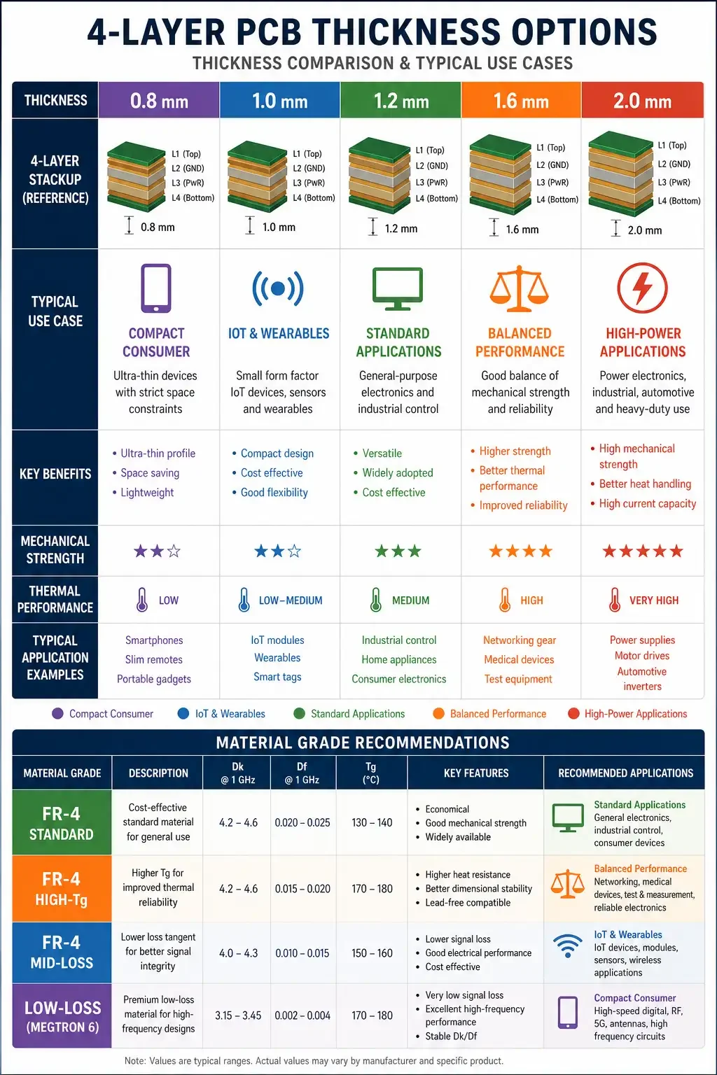
Standard FR-4
The default material for 4-layer PCBs. With Dk around 4.2–4.5 and Df around 0.020, standard FR-4 is suitable for digital designs below 100 MHz, analog circuits, and most IoT and consumer applications. It is the lowest-cost option and is available from every PCB manufacturer.
High-Tg FR-4
Required for lead-free assembly. Standard FR-4 with Tg of 130–140°C can delaminate during lead-free reflow profiles that peak above 250°C. High-Tg FR-4 with Tg of 150–170°C provides the thermal margin needed for lead-free assembly and for boards that must survive multiple reflow cycles. Use high-Tg as the default unless the assembly process is explicitly restricted to leaded profiles.
Mid-Loss FR-4
When the design includes interfaces above 100 MHz but exotic high-speed materials are not justified (such as Megtron or Rogers), mid-loss FR-4 with Df around 0.010 provides a meaningful improvement in signal loss without the cost premium of true low-loss materials. This is a good choice for 4-layer boards hosting USB 3.0, HDMI, or basic DDR3.
Copper Weight
1 oz copper (35 µm) is standard for 4-layer boards and provides good balance between trace width control, current carrying capacity, and cost. 0.5 oz copper (17.5 µm) is used when very fine geometry is required, such as for dense BGAs. 2 oz copper is occasionally used for high-current power planes but is less common on 4-layer boards.
Prepreg and Core Selection
A typical 4-layer board uses one core (two copper layers bonded to dielectric) and two prepreg sheets (uncured dielectric with no copper). The dielectric thickness between layers 1–2 and 3–4 is controlled by the prepreg stack-up; the dielectric thickness between layers 2–3 is controlled by the core thickness plus prepreg. Manufacturers have standard core and prepreg thicknesses available; customizing non-standard thicknesses adds cost and lead time.
Manufacturing Considerations
The 4-layer PCB is one of the most widely manufactured board types in the industry. Manufacturing is well-understood and yields are high. That said, a few considerations help avoid unnecessary cost or yield issues.
Symmetry
Keep the stack-up symmetric around the board center. For a 4-layer board with 1 oz copper on all layers, this is naturally the case. If you need 2 oz on the power plane, balance it with 2 oz on the ground plane to maintain symmetry and reduce warpage.
Lamination Cycle
4-layer boards are typically laminated in a single press cycle, unlike 6+ layer boards that may require multiple lamination stages. This keeps manufacturing cost lower and reduces registration tolerance stack-up.
Layer Registration
Standard layer-to-layer registration tolerance is ±0.003–0.005 inches (75–125 µm) for inner layers on 4-layer boards. Tighter registration is available but adds cost. For controlled impedance designs, registration variation affects impedance accuracy, so discuss tolerances with your manufacturer.
Panel Utilization
4-layer boards fit well into standard panel sizes (18×24 inches or 21×25 inches). For odd board sizes, work with your manufacturer on panel layout to maximize utilization. Multi-up panels (multiple boards per panel) reduce per-board cost significantly for prototypes and small batches.
Drill and Via Considerations
Standard through-hole vias are the lowest-cost option for 4-layer boards. Blind or buried vias are possible but rarely justified. Microvias (laser-drilled, used in HDI designs) are generally reserved for 6+ layer boards with BGA pitch below 0.5 mm.
Cost Considerations
The 4-layer PCB is cost-optimized for most applications, but several factors can drive unnecessary cost increases.
Material Choice
Standard FR-4 high-Tg is the cost baseline for 4-layer boards. Upgrading to mid-loss FR-4 typically adds 20–40% to material cost. Low-loss materials such as Megtron 6 can add 200–400% and are rarely justified for a 4-layer design—consider whether the design genuinely requires them, or whether a 6-layer board with low-loss inner layers would be a better investment.
Copper Weight
1 oz copper on all layers is the cost baseline. 2 oz copper adds cost and may require thicker dielectrics to maintain impedance targets. Specify 2 oz only on layers that genuinely need higher current capacity.
Impedance Tolerance
Standard ±10% impedance tolerance is included in most 4-layer board pricing. Tight tolerance (±5%) requires tighter process control and may increase cost by 10–20%. Specify the loosest tolerance that the design can tolerate.
Surface Finish
The 4-layer stack-up works with all common surface finishes (HASL, ENIG, OSP, immersion silver, immersion tin). The finish choice is independent of the stack-up and is typically driven by assembly and application requirements.
Quantity and Lead Time
4-layer boards are available with quick-turn lead times (3–5 days) at standard pricing. Volume production typically reduces per-board cost by 30–60% compared to small batches.
Step-by-Step 4-Layer PCB Design Workflow
- Define Signal Requirements: Catalog all interfaces on the board (USB, HDMI, DDR, Ethernet, analog, etc.). Note the operating frequency or data rate for each and the impedance requirements (single-ended, differential, tolerance).
- Confirm a 4-Layer Board Is Sufficient: Check whether routing density, signal count, and impedance requirements can be met on 4 layers. If high-speed buses require independent reference planes or routing density exceeds the available channels, plan for 6 or more layers.
- Choose the Stack-Up Configuration: Select S-G-P-S for general-purpose designs and G-S-S-G when inner stripline shielding is required. Most designs start with S-G-P-S.
- Select Material: Specify high-Tg FR-4 as the default for lead-free compatibility. Choose mid-loss FR-4 if operating frequencies exceed 1 GHz. Document material grade and supplier (for example, Isola FR408HR, Shengyi S1000-2M).
- Define Dielectric Thickness: Set the dielectric between layers 1–2 and 3–4 to match the trace widths required for controlled impedance on the outer layers. Use the core plus prepreg combination to achieve the thickness between layers 2–3.
- Calculate Impedance: Use a field solver with the stack-up geometry to calculate trace widths and spacings for controlled impedance nets. Confirm calculated values are within manufacturer capability.
- Design Plane Shapes: Place a continuous ground plane on layer 2. Plan the power plane on layer 3, including any splits for multiple supply voltages. Identify any signal routes that cross splits and add return path bridges.
- Review with Manufacturer: Share the preliminary stack-up with your PCB manufacturer for DFM review. Confirm material availability, dielectric thickness capability, and impedance modeling support.
- Document the Final Stack-Up: Generate a cross-sectional stack-up drawing showing layer types, copper weights, dielectric thicknesses, and material specifications. Include this in the fabrication notes and the RFQ.
- Validate Production Output: On the first production batch, request impedance test coupons and verify measured impedance against the modeled values. Adjust future orders if systematic deviations appear.
Frequently Asked Questions
What is the most common 4-layer PCB stackup?
The most common 4-layer PCB stackup is Signal–Ground–Power–Signal (S-G-P-S). Layer 1 carries top-side signals and references the ground plane on layer 2. Layer 3 is a power plane that distributes supply voltages and provides additional shielding. Layer 4 carries bottom-side signals and references the power plane. This arrangement provides a continuous return path for top-side high-speed signals, accommodates controlled impedance routing on both outer layers, and supports standard FR-4 materials.
Can a 4-layer PCB be used for controlled impedance routing?
Yes. The standard S-G-P-S arrangement supports controlled impedance microstrip on both outer layers (layer 1 referencing ground, layer 4 referencing power). For inner-layer stripline routing—where a trace sits between two reference planes—an alternate G-S-S-G arrangement is required. With accurate field-solver modeling and manufacturer verification, 4-layer boards can host USB 2.0/3.0, HDMI, DDR3, Ethernet, and similar interfaces.
Should the ground plane be on layer 2 or layer 3 in a 4-layer PCB?
The standard practice is to place the ground plane on layer 2, directly below the top signal layer on layer 1. This minimizes return current loop area for top-side high-speed signals, which is where the densest and most critical routing usually lives. Placing the ground plane on layer 3 instead is sometimes done for RF sections or analog-heavy designs where the top layer is a sensitive analog signal, but for most mixed-signal and digital designs, ground on layer 2 is the correct choice.
What is the standard thickness of a 4-layer PCB?
The most common 4-layer PCB thickness is 1.6 mm (0.063 inches). Other available thicknesses include 0.8 mm, 1.0 mm, 1.2 mm, and 2.0 mm. The total thickness depends on the dielectric distribution between layers, copper weights, and the core/prepreg combination used. Thinner boards are popular for compact consumer devices; thicker boards are used for mechanical rigidity or high-power applications.
When should I move from a 4-layer to a 6-layer PCB?
Move to a 6-layer PCB when the design exceeds 4-layer capability. Specific triggers include: routing density that cannot be resolved with two signal layers, multiple high-speed buses that each require an independent reference plane, complex power distribution that cannot be handled with a single power plane, or impedance control requirements that demand inner stripline layers while preserving dedicated power planes. For DDR4/5, PCIe, and other multi-gigabit interfaces, 6 or more layers are often the better starting point.
Is a 4-layer PCB enough for USB, HDMI, or DDR3?
A 4-layer PCB can host USB 2.0 and lower-speed interfaces with margin. USB 3.0, HDMI, and DDR3 are achievable on 4 layers with proper impedance control, a continuous ground plane on layer 2, and careful routing. DDR4, DDR5, PCIe Gen3 and above typically require 6 or more layers because the routing density and reference plane requirements exceed what a 4-layer board can provide.
References
- IPC-2221: Generic Standard on Printed Circuit Board Design
https://www.ipc.org/ - IPC-2222: Sectional Design Standard for Rigid Organic Printed Boards
https://www.ipc.org/ - IPC-4101: Specification for Base Materials for Rigid and Multilayer Printed Boards
https://www.ipc.org/ - IPC-4552: Specification for Electroless Nickel/Immersion Gold (ENIG) Finish
https://www.ipc.org/ - SMTA Surface Mount Technology Association Resources
https://www.smta.org/ - Global Electronics Association (formerly IPC) Standards Library
https://www.ipc.org/
Further Reading
- PCB Stack-Up Design — Comprehensive guide to multilayer stack-up design across all layer counts
- Controlled Impedance PCB Stackup — Detailed impedance modeling and design considerations
- Multilayer PCB Manufacturer — Manufacturing capabilities for 4-layer and higher boards
- Custom PCB Manufacturer — Selecting a supplier for your project
- PCB Copper Weight — Choosing copper thickness for signal and power layers
- PCB Surface Finish Comparison — Finish options after stack-up selection
- PCB Quote Requirements — Preparing an RFQ with your stack-up specifications
Shanghai Huangte Technology Co., Ltd. | Last updated: 2026-07-26
This article provides general technical guidance for 4-layer PCB stack-up design. Specific applications may require specialized materials or configurations. Consult with your PCB manufacturer early in design to ensure stack-up compatibility with their capabilities and your performance requirements.