Why Stack-Up Design Matters
The PCB stack-up determines how signals propagate through the board, how power distributes to components, and how the board performs thermally and mechanically. Every electrical characteristic—impedance, crosstalk, ground bounce, EMI emissions, and power distribution network impedance—traces back to decisions made in the stack-up design phase.
Signal integrity engineers often say that “60–80% of signal integrity problems originate in the stack-up, not the routing.” This is because trace geometry alone cannot compensate for missing reference planes, improper layer sequencing, or inappropriate material properties. Similarly, power integrity challenges such as voltage ripple and ground noise often result from inadequate power/ground plane design rather than insufficient decoupling capacitance.
The stack-up also constrains what is physically possible in PCB routing and manufacturing. Layer count determines routing channel availability. Substrate thickness affects trace width requirements for controlled impedance. Material selection determines thermal performance and cost. These interdependencies mean that stack-up decisions made early in design—before schematic completion—are among the most consequential.
Fundamentals of PCB Materials
Understanding material properties is essential for informed stack-up design. The key parameters are dielectric constant, dissipation factor, glass transition temperature, and coefficient of thermal expansion.
Dielectric Constant (Dk) is the ratio of a material’s permittivity to vacuum permittivity. It determines the effective capacitance between conductors and directly affects trace impedance. Standard FR-4 typically has Dk of 4.2–4.5 at 1 MHz, though the value varies with frequency and resin content. High-speed materials offer Dk values of 3.0–4.0, reducing trace widths for a given impedance and improving signal integrity at high frequencies.
Dissipation Factor (Df) measures energy loss in the dielectric material. Lower Df indicates less signal attenuation, which is critical for high-frequency and long trace applications. Standard FR-4 has Df of 0.015–0.025, while low-loss materials achieve Df below 0.005. At 5 GHz, the difference between FR-4 and low-loss material can mean several decibels of additional loss per inch.
Glass Transition Temperature (Tg) indicates the temperature at which the substrate changes from rigid to rubbery state. Standard FR-4 has Tg around 130–140°C; high-Tg FR-4 reaches 150–170°C. Lead-free assembly processes with higher peak reflow temperatures make high-Tg materials essential for boards that must survive multiple assembly cycles without delamination.
Coefficient of Thermal Expansion (CTE) describes how the material expands with temperature. CTE mismatch between copper and substrate causes stress during thermal cycling. This is particularly important for plated through-holes (vias) where cyclic stress can eventually cause barrel cracking.
Common PCB Material Families
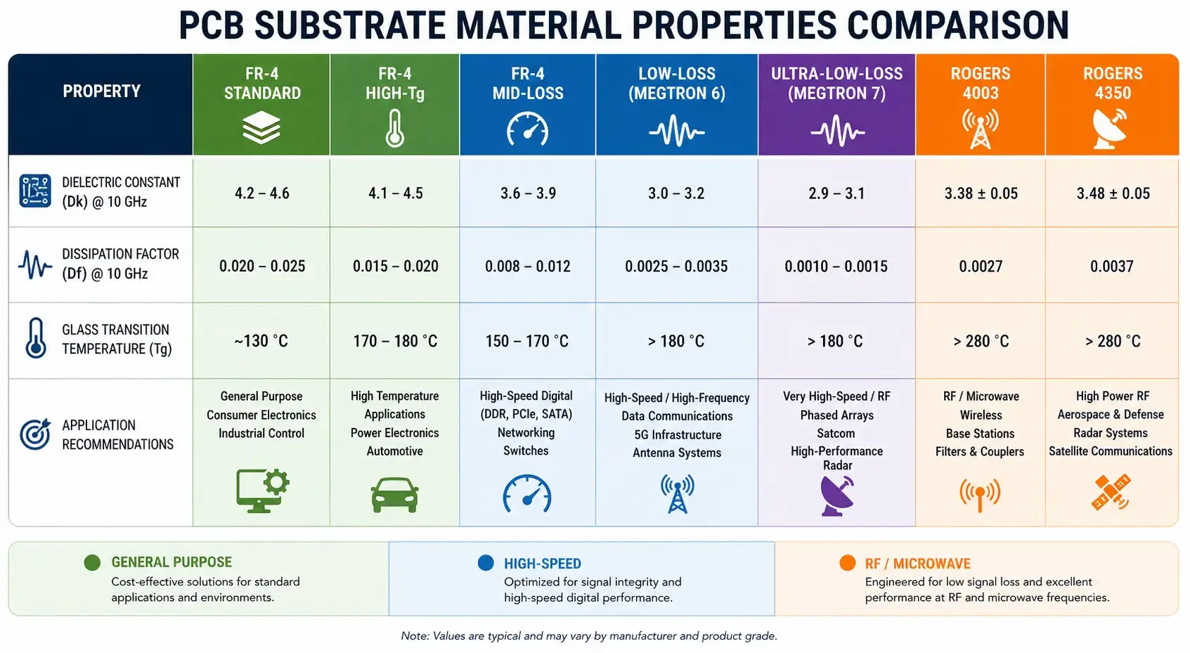
| Material | Typical Dk | Typical Df | Tg (°C) | Application |
|---|---|---|---|---|
| FR-4 Standard | 4.2–4.5 | 0.020 | 130–140 | General purpose |
| FR-4 High-Tg | 4.2–4.5 | 0.018 | 150–170 | Lead-free compatible |
| FR-4 Mid-Loss | 4.0–4.3 | 0.010 | 140–150 | Moderate speed |
| Low-Loss (Megtron 6) | 3.7 | 0.004 | 200+ | High-speed digital |
| Ultra-Low-Loss (Megtron 7) | 3.4 | 0.002 | 200+ | 10+ Gbps |
| Rogers 4003 | 3.55 | 0.0027 | N/A | RF/microwave |
| Rogers 4350 | 3.48 | 0.0037 | N/A | RF/microwave |
Standard Stack-Up Configurations
2-Layer Boards
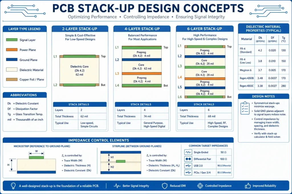
A 2-layer stack-up is the simplest configuration with copper on both sides of the substrate. While routing density is limited, 2-layer boards remain appropriate for many applications. The key design principle is to use one layer as a dedicated ground plane whenever possible, dedicating the other layer for signal routing. Without a reference plane, controlled impedance is difficult to achieve consistently.
4-Layer Boards
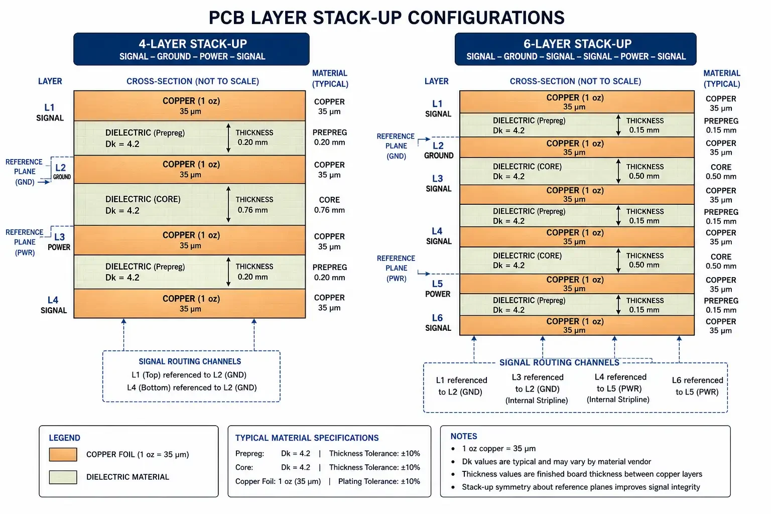
The 4-layer stack-up is the most common configuration for moderate-complexity designs. A standard 4-layer arrangement is:
| Layer | Type | Function |
|---|---|---|
| 1 | Signal | Top components, critical routing |
| 2 | Ground | Continuous ground plane |
| 3 | Power | Power distribution plane |
| 4 | Signal | Bottom routing, less critical signals |
This arrangement places the top signal layer adjacent to a ground plane, providing excellent return current path for high-speed signals. The power plane on layer 3 provides power distribution while also contributing to shielding between top and bottom signal layers.
6-Layer Boards
A 6-layer stack-up supports higher routing density and better signal integrity:
| Layer | Type | Function |
|---|---|---|
| 1 | Signal | Top components, critical signals |
| 2 | Ground | Ground reference for layer 1 |
| 3 | Signal | Inner signal routing |
| 4 | Signal/Power | Inner routing or split power |
| 5 | Power | Power distribution plane |
| 6 | Signal | Bottom routing |
8-Layer and Higher
As layer count increases, the designer has more flexibility in layer assignment. General principles include:
- Signal layers should always be adjacent to reference planes
- Ground planes should sandwich signal layers (G-S-G or G-S-S-G)
- Keep power and ground planes close together for capacitance
- Separate high-speed signal layers from low-speed with ground references
Layer Arrangement Principles
The arrangement of signal, power, and ground layers within the stack-up profoundly affects electrical performance. These principles guide layer assignment decisions.
Adjacent Reference Planes
Every signal layer should have a reference plane immediately adjacent (above or below). The reference plane provides return current path for high-frequency signals and defines trace impedance. Gaps between signal layers and their reference planes cause impedance discontinuities and increased crosstalk.
Ground Plane Sandwiching
For high-speed signals, sandwich signal layers between ground planes (G-S-G). This provides shielding that reduces both radiated emissions and susceptibility to external interference. The ground planes on both sides of the signal layer contain return currents and prevent them from coupling to adjacent signal layers.
Power and Ground Proximity
Place power and ground planes adjacent to each other wherever possible. This creates distributed capacitance that supplements decoupling capacitors, particularly at high frequencies where capacitor ESL limits effectiveness. A 0.5 oz copper power/ground pair provides approximately 40 pF per square inch of overlapping area.
Signal Layer Separation
When multiple signal layers exist, separate high-speed layers from low-speed layers with ground planes. Route critical differential pairs and clock signals on layers closest to ground references. Place lower-priority signals on outer layers where they cause minimal interference to sensitive inner layers.
Copper Weight and Distribution
Copper weight (thickness) affects trace resistance, current capacity, and manufacturing yield. Standard copper weights are 0.5 oz (17.5 µm), 1 oz (35 µm), and 2 oz (70 µm) per side.
Signal Layers: 0.5 oz or 1 oz copper is typical for signal routing. Thinner copper allows finer trace geometry and better impedance control. 1 oz is common for controlled impedance designs where manufacturing tolerances require larger trace widths.
Power Planes: Power planes typically use 1 oz or heavier copper to minimize resistance and distribute current effectively. Heavy copper (2 oz or more) is used for high-current applications such as power supply outputs.
Copper Balance: Uneven copper distribution across layers causes differential etching, where etchant flow concentrates in low-copper areas, resulting in inconsistent trace widths. Use copper fills and thermal relief patterns to balance copper density across each layer. Generally, maintain copper coverage between 20% and 80% per layer after subtracting routed signal areas.
Controlled Impedance Design
Many modern applications—DDR memory interfaces, USB, PCIe, SerDes links—require controlled impedance traces to maintain signal integrity. The stack-up design must support the required impedance values.
Microstrip is a trace on the outer layer with a reference plane below it and air above. Microstrip impedance is determined by trace width, substrate thickness (distance to reference plane), and substrate Dk. Microstrip is easier to manufacture with consistent impedance but is more susceptible to external interference.
Stripline places a trace between two reference planes within the inner layers. Stripline provides better shielding and consistent impedance but requires more complex manufacturing. Asymmetric stripline (trace closer to one reference plane) is common and requires careful modeling.
Impedance Calculation Parameters
- Target impedance (typically 50 Ω single-ended, 100 Ω differential)
- Substrate Dk at operating frequency
- Trace width and thickness
- Distance to reference plane(s)
- Tolerance requirements (±10% standard, ±5% tight)
Field solvers and specialized calculators are essential for impedance stack-up design. Input the stack-up geometry and material properties; the tool calculates required trace widths. Always verify calculations with your manufacturer, as dielectric constant values vary between material lots and suppliers.
Impedance Tolerance Considerations
Manufacturing tolerances in trace width, substrate thickness, and copper plating affect achievable impedance tolerance. Standard tolerance is ±10%; tight tolerance (±5%) requires tighter process control and may affect cost and lead time. Table the required tolerance against the application’s sensitivity—DDR5 memory typically requires ±5% or tighter, while lower-speed interfaces may tolerate ±15%.
Material Selection Guide
Material selection integrates electrical requirements, thermal requirements, availability, and cost.
For General-Purpose Digital Designs (up to 100 MHz)
Standard FR-4 meets requirements at lowest cost. Specify high-Tg if lead-free assembly is required. Verify that dissipation factor does not limit performance for longer traces or higher speeds.
For High-Speed Digital (1–10 Gbps)
Low-loss materials such as Megtron 6 or Panasonic Megtron 7 provide better signal integrity. These materials reduce attenuation at high frequencies and support longer trace lengths without equalization. Cost premium is 2–4× standard FR-4.
For RF and Microwave Applications
Rogers materials (RO4003, RO4350) offer tight Dk tolerance (±0.05), low loss, and excellent high-frequency performance. These materials require different processing than FR-4 and typically command 5–10× cost premium.
For High-Temperature Applications
Polyimide or high-Tg materials are required when boards must survive temperatures above standard assembly profiles. Polyimide offers superior thermal resistance but higher cost and more difficult processing.
Material Availability Constraints
Not all material types are available in all thickness and panel sizes. Consult with your manufacturer early in design to confirm that preferred materials are producible in your required format. Some exotic materials require extended lead times or minimum order quantities.
Manufacturing Constraints
Stack-up design must account for manufacturing realities to avoid yield issues or requotes.
Panel Utilization: PCB manufacturers produce boards on standard panel sizes (typically 18×24 inches or 21×25 inches). Stack-ups with odd-layer counts may waste panel space or require non-standard panel sizes. Discuss panel optimization with your manufacturer early.
Layer Registration: As layer count increases, the tolerance stack-up for layer-to-layer alignment becomes more challenging. Standard tolerance is ±0.003–0.005 inches for inner layers; tighter tolerance requires controlled impedance testing on production boards.
Via Types: Through-holes, blind vias, and buried vias have different manufacturing requirements and costs. Through-holes are standard and lowest cost. Blind and buried vias enable higher routing density but increase complexity and cost. Via-in-pad requires filled and capped vias.
Minimum Feature Sizes: Trace width, spacing, and annular ring requirements depend on PCB class (IPC-2221 Class 1, 2, or 3) and manufacturer capabilities. Request your manufacturer’s design rules and design within their capabilities.
Cost vs Performance Trade-Offs
Stack-up cost increases with layer count, exotic materials, and tight tolerances. The goal is meeting requirements at minimum cost, not maximizing performance beyond what the application demands.
Layer Count Optimization: Each additional layer adds cost and lead time. Evaluate whether routing density genuinely requires additional layers, or whether better placement and routing optimization on existing layers could eliminate the need. Often, a 4-layer design can accommodate a 6-layer design’s functionality through careful planning.
Material Grade Selection: Standard FR-4 handles most applications below 1 GHz. Avoid specifying exotic materials if standard materials meet electrical requirements. The cost and lead-time premium for low-loss materials is only justified when signal integrity benefits outweigh cost.
Tolerance Relaxation: Specify the loosest impedance tolerance that the application can tolerate. Standard ±10% tolerance is achievable with lower process control requirements and higher yield. Reserve tight tolerances for interfaces that genuinely require them.
Panel Efficiency: Work with your manufacturer to optimize panel utilization. Sharing panel space with other designs (multi-up panels) can significantly reduce per-board cost.
Step-by-Step Stack-Up Design Workflow
- Define Requirements: Document signal types (single-ended, differential), speed/frequency, impedance targets, power distribution needs, thermal requirements, and regulatory constraints (IPC class, UL rating).
- Estimate Layer Count: Based on routing density, power distribution complexity, and shielding requirements, estimate minimum layer count. Add margin for routing flexibility.
- Select Materials: Choose material family based on frequency/speed requirements, thermal requirements, and cost constraints. Document Dk and Df values for impedance calculations.
- Define Preliminary Stack-Up: Assign layers as signal/power/ground. Apply layer arrangement principles. Calculate approximate thicknesses.
- Calculate Impedance Targets: Using stack-up geometry and material properties, calculate trace widths for controlled impedance traces. Verify that calculated widths are within manufacturing capability.
- Review with Manufacturer: Share preliminary stack-up with your PCB manufacturer for producibility review. Incorporate their feedback on material availability, minimum features, and cost optimization.
- Finalize Stack-Up Documentation: Document the final stack-up including all layer assignments, thicknesses, material properties, and impedance targets. This documentation enables controlled impedance testing and quality verification.
- Create Stack-Up Drawing: Generate a manufacturing drawing showing cross-sectional stack-up with all layer thicknesses, copper weights, and material specifications. This drawing becomes part of the production data package.
Frequently Asked Questions
How many layers do I need for a DDR4 memory interface?
DDR4 interfaces typically require 6–8 layers minimum. The tight timing margins of DDR4 demand excellent signal integrity, which requires solid reference planes adjacent to all high-speed signal layers. A typical DDR4 stack-up might be: Signal-Ground-Signal-Power-Signal-Ground-Signal, with tight impedance control (±5%) on the address/command and data signals.
What is the best stack-up for PCIe Gen4 or Gen5?
PCIe Gen4 and Gen5 require 8–10 layers at minimum. These high-speed serial interfaces need controlled impedance of 85 Ω differential (±5%), low-loss materials (Df < 0.01), and careful via design. Ground reference planes must be continuous beneath all high-speed traces. Many designs use hybrid stack-ups with standard FR-4 for outer layers and low-loss materials for inner high-speed layers.
How does substrate thickness affect controlled impedance?
Substrate thickness (distance from trace to reference plane) is the primary determinant of trace width for a given impedance. Thinner substrates allow narrower traces but are more sensitive to manufacturing variations. For 50 Ω microstrip on FR-4, typical thickness is 4–5 mil to dielectric for 1 oz copper, requiring trace widths of approximately 5–7 mil.
Should I use symmetric or asymmetric stack-up?
Symmetric stack-ups (identical construction above and below the center) are preferred for boards that will be surface-mounted, as symmetric CTE reduces warpage during assembly reflow. Asymmetric stack-ups are acceptable for boards without surface mounting or where routing requirements favor uneven layer distribution. Minimize asymmetry when possible.
What is the minimum spacing between signal layers?
Signal layers should be separated by reference planes whenever possible. When routing on adjacent signal layers is unavoidable (due to high layer count), route orthogonally (one layer horizontal, one vertical) and maintain maximum separation. Use ground stripline techniques where inner signal layers are between ground planes.
References
- IPC-2221: Generic Standard on Printed Circuit Board Design
https://www.ipc.org/ - IPC-2152: Standard for Determining Current Carrying Capacity in Printed Circuit Board Design
https://www.ipc.org/ - IPC-4101: Specification for Base Materials for Rigid and Multilayer Printed Boards
https://www.ipc.org/ - IPC-4412: Specification for High Frequency Laminates
https://www.ipc.org/
Further Reading
- Custom PCB Manufacturer — Finding a supplier for your stack-up requirements
- Multilayer PCB Manufacturer — Manufacturing capabilities for complex stack-ups
- PCB Surface Finish Comparison — Coordinating finish selection with stack-up design
- PCB Quote Requirements — Documenting stack-up specifications in your RFQ
Shanghai Huangte Technology Co., Ltd. | Last updated: 2026-07-21
This article provides general technical guidance for PCB stack-up design. Specific applications may require specialized materials or configurations. Consult with your PCB manufacturer early in design to ensure stack-up compatibility with their capabilities and your performance requirements.