Why Controlled Impedance Matters
Signal integrity failures cause some of the most difficult problems in high-speed PCB design. When signals travel faster than approximately 100 Mbps, the trace geometry on your board begins to behave as a transmission line rather than a simple wire. Without controlled impedance design, signals reflect at discontinuities, causing eye diagram degradation, timing errors, electromagnetic interference, and system failures that are difficult to debug.
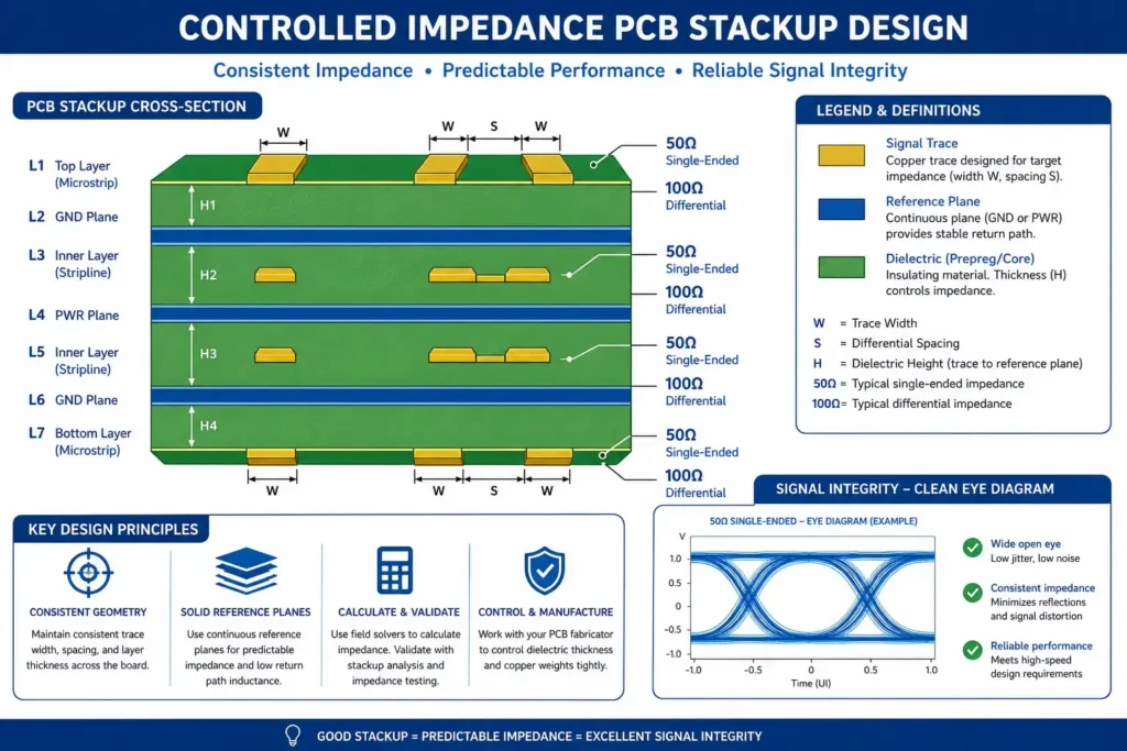
A controlled impedance PCB stackup ensures that signal traces maintain consistent impedance throughout their routing, from source to destination. The characteristic impedance—typically 50Ω for single-ended signals or 90-100Ω for differential pairs—is determined by the physical stack-up geometry: trace width, trace thickness, substrate height, and dielectric constant. When any of these parameters vary beyond tolerance, impedance shifts, creating reflections that corrupt signal quality.
Industries relying on high-speed interfaces—computing, communications, automotive, aerospace—require controlled impedance design as a baseline requirement. USB 3.0, PCIe Gen 3/4/5, DDR4/DDR5 memory, and 10+ Gbps Ethernet all demand tight impedance control to function reliably. The cost of impedance-related failures—board respins, field failures, warranty claims—far exceeds the modest investment in proper controlled impedance design upfront.
Impedance Fundamentals
Characteristic impedance (Z0) represents the ratio of voltage to current for a wave propagating along a transmission line. For PCB traces, Z0 depends on the trace geometry and surrounding dielectric materials. The fundamental relationship is:
Z0 = (87 / √(Dk + 1.41)) × ln(5.98 × H / (0.8 × W + T))
Where Dk is the dielectric constant of the substrate material, H is the substrate height (distance to reference plane), W is trace width, and T is trace thickness.
Three key principles govern controlled impedance design. First, every high-speed signal trace requires an adjacent reference plane—ground or power—to define its impedance. Second, impedance consistency matters more than achieving a specific target value; a trace that varies from 48Ω to 52Ω causes more problems than a trace consistently at 51Ω. Third, all impedance-related parameters must be controlled within tolerance stack-up to maintain consistency across the board and between production panels.
Dielectric constant (Dk) varies with frequency, temperature, and material composition. Standard FR-4 typically has Dk of 4.2-4.5 at 1 MHz, but this value decreases at higher frequencies and varies between manufacturers and material lots. For controlled impedance designs, specify Dk at your operating frequency and account for typical variation of ±5%.
Microstrip vs Stripline
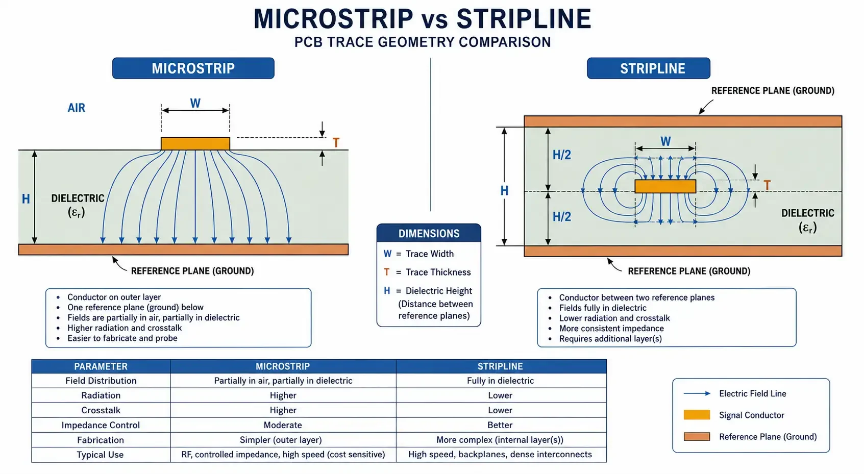
Two primary transmission line geometries exist for controlled impedance PCBs: microstrip and stripline. Each offers distinct advantages and trade-offs.
Microstrip places the signal trace on an outer layer with a reference plane below it and air above. This geometry is simpler to manufacture and access for testing. Microstrip traces radiate more readily, making them susceptible to external interference but also useful for antenna feeds and controlled radiation applications. Microstrip is the standard choice for most controlled impedance applications on outer layers.
Stripline routes the signal trace between two reference planes within the inner layers of the board. The trace is completely enclosed by dielectric material, providing superior shielding against external interference and containing electromagnetic radiation within the board. Stripline is preferred for ultra-high-speed applications where signal isolation is critical, but it requires more complex stack-up design and is more difficult to modify or debug.
| Characteristic | Microstrip | Stripline |
|---|---|---|
| Manufacturing complexity | Lower | Higher |
| Impedance control | Good | Excellent |
| EMI shielding | Moderate | Excellent |
| Test accessibility | Easy | Difficult |
| Typical application | USB, HDMI, Ethernet | PCIe, high-speed SerDes |
For most designs, a hybrid approach works best: use microstrip for critical signals on outer layers and stripline for sensitive inner-layer routing where isolation is required.
Single-Ended vs Differential Impedance
Single-ended impedance measures the characteristic impedance of a single trace referenced to ground. The 50Ω single-ended standard emerged from early RF and microwave design and remains dominant for most high-speed digital interfaces including USB, HDMI, and SATA.
Differential impedance measures the impedance between two complementary signals traveling as a pair. The signals are routed together with tight spacing, and the differential impedance is the impedance that the pair presents to differential signaling. Common differential impedance standards include 100Ω (USB 3.0, Ethernet), 90Ω (PCIe), and 85Ω (SATA).
Differential signaling offers several advantages over single-ended: common-mode noise rejection, reduced electromagnetic emissions, and doubled signal voltage swing with lower voltage levels. These benefits come at the cost of tighter routing constraints—differential pairs require consistent spacing and length matching.
| Interface Type | Single-Ended Impedance | Differential Impedance |
|---|---|---|
| USB 3.0 | 45-55Ω | 90-110Ω |
| PCIe Gen 3/4 | 45-55Ω | 85-95Ω |
| Ethernet (1000BASE-T) | 50Ω | 100Ω |
| SATA | 45-55Ω | 85-100Ω |
| DDR4/DDR5 | 40-50Ω | 80-120Ω |
For differential pair design, maintain consistent coupling (spacing) throughout the routing and match trace lengths to within tight tolerances (typically 5-10 mil for high-speed interfaces). Avoid vias and maintain symmetry in the pair geometry.
Stack-Up Parameters for Impedance Control
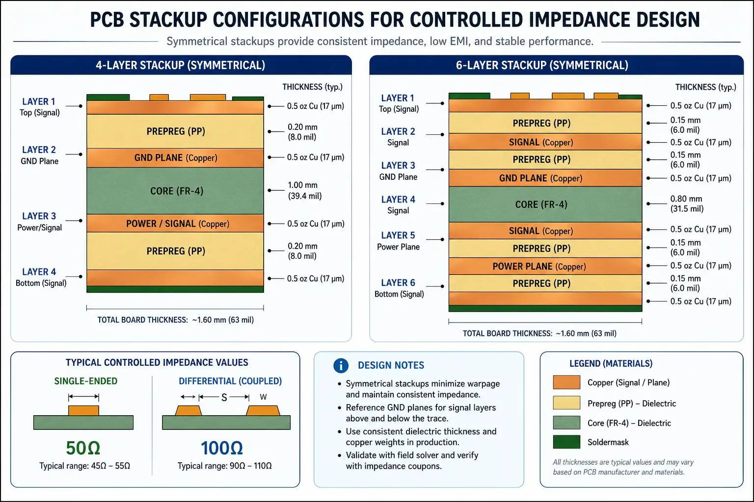
Designing a controlled impedance stack-up requires balancing multiple parameters. The key variables are:
Trace Width (W): Wider traces produce lower impedance for a given geometry. Trace width tolerance is typically ±0.5-1 mil for controlled impedance designs, contributing to impedance variation. Standard PCB manufacturing can achieve 4-6 mil minimum trace widths; tighter tolerances require specialized processing.
Trace Thickness (T): Copper weight determines trace thickness. For controlled impedance, 0.5 oz (0.7 mil) or 1 oz (1.4 mil) copper is typical. Plating adds thickness to outer layer traces, which must be accounted for in calculations. Specify finished copper weight rather than starting weight.
Substrate Height (H): The distance from trace to reference plane is the primary determinant of impedance. Thinner dielectrics allow narrower traces but are more sensitive to thickness variation. For 50Ω microstrip on FR-4, substrate heights of 4-8 mil are common, requiring trace widths of approximately 5-10 mil.
Dielectric Constant (Dk): Material selection determines Dk. Standard FR-4 has Dk of 4.2-4.5, while high-speed materials offer Dk values of 3.0-4.0. Lower Dk materials allow narrower traces for the same impedance. Always specify Dk at your operating frequency.
Coverlay/Solder Mask: Outer layer traces are covered by solder mask or coverlay, which adds dielectric thickness above the trace. This affects microstrip impedance and must be included in calculations. Typical solder mask thickness is 0.5-1 mil with Dk of approximately 3.5.
Impedance Calculations
Accurate impedance calculation requires either empirical formulas, 2D field solvers, or 3D electromagnetic simulation. For preliminary design, the microstrip formula provided earlier provides reasonable estimates. For production designs, use a field solver tool from your PCB manufacturer or a third-party tool such as Polar Instruments Si9000 or Sunlord’s calculator.
When calculating impedance, account for manufacturing tolerances in your stack-up parameters:
- Dk variation: ±5% typical for FR-4
- Substrate thickness: ±10% typical
- Trace width: ±0.5-1 mil typical
- Copper plating: ±0.3 mil typical
- Etch compensation: Varies by line/space ratio
The total impedance tolerance is the root-sum-square of individual tolerances. For a stack-up with ±5% Dk, ±10% thickness, and ±1 mil trace width variation, total tolerance can exceed ±15%, which exceeds the ±10% requirement for standard controlled impedance.
For critical applications requiring ±5% tolerance, you must work closely with your manufacturer to define stack-up parameters that can achieve tight tolerance. This may require tighter material specifications, special inspection processes, or selection of manufacturers with better process control.
Manufacturing Tolerances
Standard controlled impedance tolerance is ±10%, achievable by most manufacturers with standard processes. Tight tolerance of ±5% is required for DDR4/DDR5, PCIe Gen 4/5, and other advanced interfaces. Achieving ±5% requires specialized manufacturing controls and may affect cost and lead time.
Manufacturers use several methods to control impedance:
- Coupon testing: Test traces on production panels are measured using TDR to verify impedance
- In-process monitoring: Sampling during production to catch drift
- Cross-section analysis: Destructive testing of samples to verify physical parameters
- Design for Manufacturability (DFM) feedback: Manufacturer suggests stack-up modifications to achieve target tolerance
Always request impedance reports from your manufacturer, especially for critical designs. These reports document measured impedance on your production panels and verify conformance to specifications.
Stack-Up Design Examples
4-Layer Controlled Impedance Stack-Up
A common 4-layer configuration for controlled impedance designs:
| Layer | Type | Thickness | Purpose |
|---|---|---|---|
| 1 | Signal | 1.4 mil Cu | Microstrip traces |
| 2 | Ground Plane | Full plane | Reference for L1 and L3 |
| 3 | Power Plane | Split planes | Power distribution |
| 4 | Signal | 1.4 mil Cu | Microstrip traces |
This stack-up supports 50Ω single-ended and 100Ω differential impedance for USB, Ethernet, and similar interfaces. Ground plane adjacent to both signal layers provides return current path and shielding.
6-Layer Controlled Impedance Stack-Up
For more complex designs requiring both microstrip and stripline routing:
| Layer | Type | Thickness | Purpose |
|---|---|---|---|
| 1 | Signal | 1.4 mil Cu | Microstrip, critical signals |
| 2 | Ground Plane | Full plane | Reference for L1 |
| 3 | Signal Inner | 1.4 mil Cu | Stripline routing |
| 4 | Signal Inner | 1.4 mil Cu | Stripline routing |
| 5 | Power Plane | Split planes | Power distribution |
| 6 | Signal | 1.4 mil Cu | Microstrip, less critical |
This configuration provides two stripline layers for high-speed differential pairs (DDR, PCIe) and outer microstrip for USB, HDMI, and other connector-interface signals.
Controlled Impedance Verification
Verification ensures your manufactured boards meet impedance specifications:
TDR Testing: Time Domain Reflectometry sends a fast edge down the trace and measures reflections. Impedance discontinuities appear as reflections. TDR is the standard production test method for controlled impedance verification.
Test Coupons: Dedicated impedance test structures are included on each production panel. These coupons are manufactured with the same stack-up as production traces and are tested using TDR. Coupon results represent the impedance of production traces.
Cross-Section Analysis: For first article qualification, boards are cross-sectioned to measure actual trace geometry. Substrate height, trace width, and copper thickness are measured under microscope. These measurements confirm stack-up parameters match design intent.
Impedance Reports: Request impedance reports from your manufacturer documenting coupon test results for each production panel. Reports should include measured impedance values, tolerance, and test equipment calibration.
Common Mistakes and Solutions
Missing Reference Plane: Every controlled impedance trace requires an adjacent reference plane. Traces over split power planes, over gaps in ground, or without any adjacent plane will not achieve target impedance. Solution: Ensure continuous reference plane adjacent to all controlled impedance traces.
Ignoring Solder Mask: Designers sometimes calculate impedance for bare dielectric and ignore solder mask effects. Solder mask adds dielectric above the trace and affects impedance. Solution: Include solder mask in impedance calculations or specify impedance for “with solder mask” condition.
Using Starting Copper Weight: Impedance calculations must use finished copper thickness, not starting weight. Plating adds copper to outer layers. Solution: Specify finished copper weight and provide impedance calculations based on finished dimensions.
Assuming Uniform Dk: FR-4 Dk varies with frequency, temperature, and between material lots. Solution: Specify Dk at your operating frequency and account for typical variation.
Tight Tolerance Without Manufacturer Input: Specifying ±5% tolerance without consulting your manufacturer may result in unmanufacturable designs. Solution: Engage manufacturer early to confirm achievable tolerances for your stack-up.
Frequently Asked Questions
What is the standard impedance for PCBs?
The most common single-ended impedance is 50Ω, used for USB, HDMI, Ethernet, and most high-speed digital interfaces. Differential impedance standards include 100Ω for USB and Ethernet, 90Ω for PCIe, and 85Ω for SATA. Custom impedance values are possible with manufacturer coordination but are less common.
What’s the difference between microstrip and stripline?
Microstrip places the signal trace on an outer layer with ground below and air above. It is simpler to manufacture and test. Stripline routes signals between two ground planes in inner layers, providing better shielding and impedance control. Most designs use both: microstrip for connector-interface signals and stripline for internal high-speed routing.
How tight should controlled impedance tolerance be?
Standard tolerance is ±10%, sufficient for most applications including USB 2.0 and 10/100 Ethernet. Tight tolerance of ±5% is required for DDR4/DDR5 memory, PCIe Gen 3/4/5, and other advanced interfaces. Work with your manufacturer to determine achievable tolerance for your specific stack-up.
What affects controlled impedance accuracy?
Material Dk variation (typically ±5% for FR-4), trace width tolerance (±0.5-1 mil), substrate thickness variation (±10%), copper plating uniformity, and etch factor all affect impedance accuracy. The total tolerance is the root-sum-square of individual variations. Specify tolerances appropriate for your application.
How is controlled impedance verified?
Controlled impedance is verified using TDR (Time Domain Reflectometry) testing of dedicated test coupons on production panels. For first articles, cross-section analysis measures actual trace geometry. Always request impedance reports from your manufacturer documenting test results.
Can I route controlled impedance on inner layers?
Yes, inner layers can support controlled impedance using stripline geometry where the trace is between two reference planes. Inner layer controlled impedance requires careful stack-up design and is more difficult to modify or debug, but it provides superior signal isolation for critical nets.
References
- IPC-2221: Generic Standard on Printed Circuit Board Design
https://www.ipc.org/ - IPC-4101: Specification for Base Materials for Rigid and Multilayer Printed Boards
https://www.ipc.org/ - SMTA: Surface Mount Technology Association Technical Resources
https://www.smta.org/ - IPC-4412: Specification for High Frequency Laminates
https://www.ipc.org/
Further Reading
- PCB Stack-Up Design: How to Coordinate Materials, Impedance and Manufacturability — General stack-up design principles
- Custom PCB Manufacturer — Finding a supplier for controlled impedance PCBs
- PCB Surface Finish Comparison — Finish selection for controlled impedance boards
- Multilayer PCB Manufacturer — Manufacturing capabilities for complex stack-ups
Shanghai Huangte Technology Co., Ltd. | Last updated: 2026-07-22
This article provides general technical guidance for controlled impedance PCB stack-up design. Signal integrity requirements vary by application and operating conditions. Consult with your PCB manufacturer early in design to ensure stack-up compatibility with their capabilities and your impedance requirements.