What Is HDI PCB Technology?
HDI PCB technology refers to a class of printed circuit board constructions that achieve higher interconnect density through smaller features, finer trace and space geometries, and advanced via structures including microvias, buried vias, and blind vias. HDI boards are defined by the use of microvias—typically 150 μm or smaller in diameter—formed by laser drilling rather than mechanical drilling.
The density advantage allows designers to place components closer together, reduce board size, improve electrical performance, and support packages with high I/O count and fine pitch. HDI is standard in smartphones, tablets, wearable devices, medical implants, aerospace electronics, and other products where miniaturization and high performance are critical.
Core HDI Features
An HDI board is distinguished by several technical characteristics that differentiate it from conventional multilayer boards:
Microvias are the defining feature of HDI technology. These vias are typically 100–150 μm in diameter, formed by laser ablation, and filled or capped to create connections between adjacent layers or across thin dielectrics. Microvias cannot span more than a few layers, so HDI designs require careful layer stacking and via stacking strategies.
Finer trace geometries on HDI boards typically support minimum line/space of 75/75 μm or tighter, compared to 100/100 μm or broader on standard boards. This enables higher routing density and more efficient use of board real estate.
Buildup construction is the layering strategy used to build up the board. Common HDI constructions include 1+N+1 (one buildup layer on each side of the core), 2+N+2 (two buildup layers on each side), and more complex stacked configurations. Each additional buildup layer adds manufacturing steps and cost.
Buried vias are vias that connect internal layers but are not visible on the outer surfaces. Buried vias are standard in HDI designs and require sequential lamination—building up the board in multiple press cycles rather than a single lamination.
HDI vs Standard Multilayer PCB
The primary difference between HDI and standard multilayer boards lies in the manufacturing process and feature resolution. Standard multilayer boards use mechanical drilling for all vias and typically support minimum line/space of 100 μm or larger. HDI boards use laser drilling for microvias, require finer imaging and etching tolerances, and often involve sequential lamination cycles.
For a designer, the practical implications include tighter design rules, higher per-layer costs, and greater sensitivity to material and process variations. The cost premium is justified when the product requires miniaturization, high-speed signals, or dense component placement that cannot be achieved with standard board technology.
HDI PCB Cost Drivers
HDI PCB cost is influenced by multiple factors. Understanding each driver helps designers estimate budgets, negotiate with manufacturers, and optimize designs for cost without sacrificing performance.
Layer Count and HDI Buildup Type
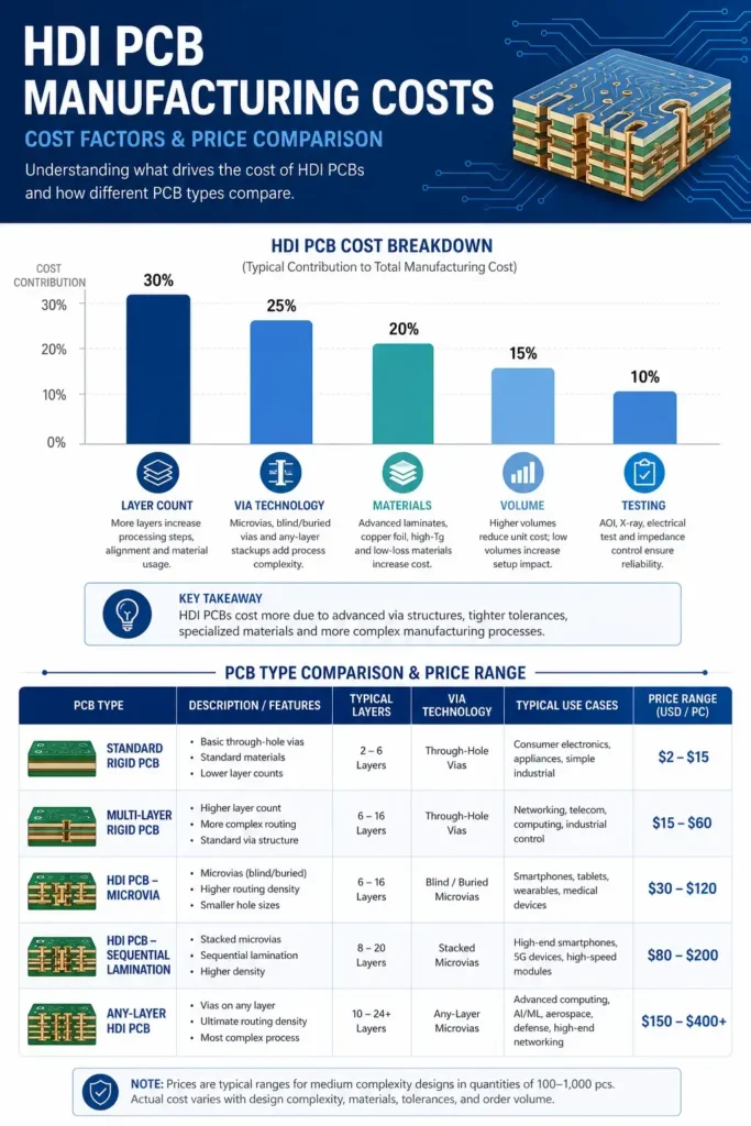
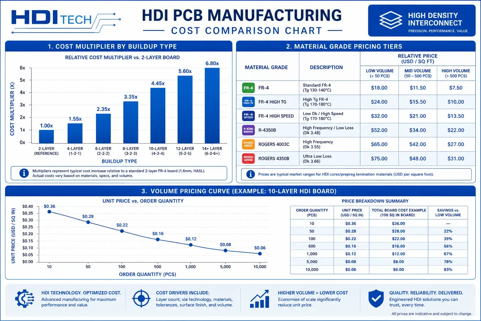
The number of layers and the HDI buildup construction are the most significant cost drivers. A simple 4-layer board with 1+N+1 HDI on the outer layers costs moderately more than a standard 4-layer board. A complex 8+ layer board with 2+N+2 or 3+N+3 buildup can cost two to five times as much as an equivalent standard multilayer board.
| HDI Construction | Description | Relative Cost | Typical Applications |
|---|---|---|---|
| 1+N+1 | 1 buildup layer on each side of core | 1.2–1.8× standard | Smartphones, tablets, IoT devices |
| 2+N+2 | 2 buildup layers on each side | 1.5–2.5× standard | Wearables, medical devices |
| 3+N+3 or any-layer | 3+ buildup layers, any-layer connectivity | 2.0–5.0× standard | Advanced smartphones, networking equipment |
The any-layer (AL) HDI construction provides full interconnectivity between any two layers using stacked microvias. This is the most advanced and expensive HDI construction, used in flagship smartphones where maximum routing flexibility is required.
Via Technology and Complexity
The type and density of vias directly affect manufacturing cost. Laser microvias require specialized equipment and process control. Filled and capped microvias add additional steps. Stacked microvias (multiple microvias stacked on top of each other to connect multiple layers) require precise alignment and additional plating.
Via-related cost factors include:
Microvia count — Each microvia requires laser drilling, desmear, and plating. Designs with hundreds of microvias cost more than those with dozens.
Via filling and capping — Filled vias (where the via barrel is filled with copper or non-conductive material) and capped vias (where the filled via is covered with a copper cap) add process steps and cost. Via-in-pad construction often requires filling.
Via stacking vs staggering — Stacked microvias (directly on top of each other) are more complex to manufacture than staggered microvias (offset between layers) and require tighter registration tolerance.
Buried via count — Internal buried vias require sequential lamination, adding cost with each additional lamination cycle.
Board Size and Panel Utilization
Board size determines how many boards fit on a standard manufacturing panel. Larger boards use more material and may reduce panel utilization if the board does not tile efficiently. Smaller boards that tile well on the panel can achieve better material utilization and lower per-board costs.
Standard HDI manufacturing panels are typically 18×24 inches or 21×24 inches. A design that fits four boards per panel will have a lower per-board setup cost than one that fits only one board per panel.
Material Selection
Material cost varies significantly by grade. Standard FR-4-compatible HDI materials are the most economical. Mid-loss and low-loss materials for high-frequency applications carry a cost premium. High-Tg and thermal-resistant materials for lead-free assembly or high-temperature environments add cost.
Material-related cost factors:
Laminate grade — Standard halogen-free FR-4-compatible HDI materials offer the best cost-to-performance ratio for most applications. Mid-loss materials (Df 0.006–0.010) cost approximately 20–40% more. Low-loss materials (Df < 0.006) cost 50–100% more.
Prepreg and buildup film — HDI constructions often use laser-drillable prepreg or buildup film rather than standard prepreg. These materials cost more than conventional prepreg.
Copper weight — Standard outer layer copper is 1 oz (35 μm). Heavier copper for power distribution adds cost and may affect microvia reliability.
Order Quantity and Volume Economics
Volume has the largest impact on per-board cost after design complexity. HDI manufacturing involves substantial setup costs including drilling programs, lamination tooling, imaging, and inspection. These setup costs are amortized across the number of panels or boards produced.
Prototype and NRE costs — A single prototype board carries the full setup cost. Prototype HDI boards typically cost $500–$2,000 depending on complexity, compared to $50–$200 for standard prototype boards.
Production volumes — At higher volumes (100+ panels), the per-panel cost drops substantially as setup costs are spread across more units. Volume pricing typically shows steep initial discounts that level off as the manufacturer approaches capacity constraints.
Panel vs piece pricing — Manufacturers typically quote panel pricing, not per-board pricing. Understanding panel utilization helps designers compare quotes accurately.
Tolerance and Test Requirements
Tighter tolerances for impedance control, registration, and dimensional accuracy add cost through additional process control, inspection, and potential yield loss. Test requirements also affect cost:
Electrical test — All boards should be tested for opens and shorts. Impedance testing adds cost per panel.
Automated optical inspection (AOI) — AOI is standard for fine-feature HDI boards to detect defects in trace geometry and solder mask.
X-ray inspection — X-ray may be required for BGA packages, buried via verification, or quality assurance on complex HDI boards.
Cross-section analysis — This destructive test verifies microvia quality, plating, and layer registration. It is typically performed on qualification prototypes rather than production boards.
Typical HDI PCB Cost Ranges
The following ranges are estimates based on typical HDI manufacturing capabilities. Actual costs depend on specific design parameters, material choices, and manufacturer capabilities.
| Board Type | Layers | Size | Quantity | Est. Cost per Panel |
|---|---|---|---|---|
| Standard rigid | 4 | 100×100 mm | 10 panels | $80–$200 |
| 1+N+1 HDI | 4 | 100×100 mm | 10 panels | $200–$500 |
| 1+N+1 HDI | 6 | 100×100 mm | 10 panels | $300–$700 |
| 2+N+2 HDI | 8 | 100×100 mm | 10 panels | $500–$1,200 |
| Any-layer HDI | 8–10 | 70×100 mm | 10 panels | $800–$2,000 |
| Any-layer HDI | 8–10 | 70×100 mm | 50 panels | $400–$1,000 |
These estimates exclude surface finish, testing, and assembly. Surface finish costs range from $30–$100 per panel depending on the finish type (HASL, ENIG, ENEPIG, etc.). Electrical test typically adds $20–$50 per panel.
Cost Reduction Strategies
Designers can take several steps to manage HDI PCB cost without sacrificing product performance:
Optimize the HDI Buildup
Choose the simplest HDI construction that meets the design requirements. If 1+N+1 satisfies routing density needs, do not specify 2+N+2. If standard microvia staggering works, avoid stacked microvias unless required for routing.
Minimize Buried Via Layers
Each additional lamination cycle adds cost and risk. Minimize the number of buried via layers. If possible, route signals on outer layers where access is easier and cost is lower.
Use Standard Materials When Possible
Select standard halogen-free HDI materials unless the application specifically requires mid-loss or low-loss performance. Standard materials have the broadest manufacturing base, shortest lead times, and lowest cost.
Optimize Panel Utilization
Work with the manufacturer to optimize board tiling on the standard panel. A design that fits six boards per panel instead of four reduces per-board cost by approximately 33%.
Design for Manufacturability
Follow the manufacturer’s DFM guidelines for minimum line/space, via size, via spacing, and annular ring. Designs that push manufacturing limits may incur premium pricing or yield loss. Early DFM review prevents costly respins.
Plan for Volume
If the product will reach production volumes, communicate this to the manufacturer early. Prototype and pre-production tooling can be amortized into production pricing. Designing for manufacture from the start avoids costly redesigns.
HDI vs Standard PCB: When Is HDI Worth the Cost?
HDI technology is justified when the design requires:
- Miniaturization — The board must fit in a smaller space than a standard board would allow.
- High I/O density — Fine-pitch BGAs, chip-scale packages, or area-array components require fine routing and microvia fan-out.
- High-speed signals — Shorter interconnects and controlled impedance on thin dielectrics improve signal integrity.
- Weight reduction — Thinner boards and fewer layers reduce weight in portable and aerospace applications.
- Improved electrical performance — Lower inductance from microvias and reduced loop area benefit power distribution and RF circuits.
For applications where standard multilayer board technology meets the design requirements, HDI is not cost-justified. A standard 6-layer board costs less than an equivalent 1+N+1 HDI 4-layer board and may provide adequate routing density.
Working with an HDI PCB Manufacturer
Selecting the right manufacturer is critical for HDI projects. Not all PCB shops have HDI capability, and those that do have varying levels of expertise and equipment.
Evaluate Manufacturing Capabilities
Ask potential manufacturers about:
- Laser drilling equipment — What via diameters and aspect ratios can they produce?
- Registration tolerance — What is their typical layer-to-layer registration tolerance?
- Buildup process — Do they use sequential lamination, and how many buildup layers can they handle?
- Materials — What HDI materials do they stock, and can they source specialty materials?
- Testing — What test capabilities do they offer (flying probe, bed-of-nails, impedance, X-ray)?
Provide Complete Design Data
Submit complete manufacturing data including:
- Gerber files for all layers
- Drill file (NC format) with plating information
- Stack-up specification with target thicknesses and impedances
- Material specifications (IPC-4101 slash-sheet or equivalent)
- Surface finish requirement
- Test requirements
- Quantity and delivery schedule
Review the PCB prototype manufacturing process for guidance on preparing files for prototype HDI boards.
Request DFM Feedback
Ask the manufacturer to review the design for manufacturability before production. A DFM review can identify issues that would cause yield loss, delays, or cost increases. For complex HDI designs, a prototype run to validate the design and manufacturing process is often worth the investment.
HDI PCB Cost vs Performance Trade-offs
Designers face several trade-offs when optimizing HDI designs for cost and performance:
| Trade-off | Lower Cost Option | Higher Performance Option |
|---|---|---|
| Via type | Staggered microvias | Stacked microvias |
| Buildup | 1+N+1 | 2+N+2 or any-layer |
| Material | Standard halogen-free | Mid-loss or low-loss |
| Tolerance | Standard | Tight impedance or registration |
| Testing | Basic electrical test | Full AOI, impedance test, X-ray |
The optimal trade-off depends on the product requirements. A consumer wearable may accept wider tolerances in exchange for lower cost. A medical device may require tight impedance control and extensive testing regardless of cost.
Frequently Asked Questions
Why does HDI PCB cost more than standard PCB?
HDI PCB cost is higher due to additional manufacturing steps including laser microvia drilling, sequential lamination for buried vias, finer imaging and etching tolerances, and specialized materials. Each microvia requires individual laser drilling and subsequent desmear and plating steps. The setup and tooling costs for HDI are also higher than for standard multilayer boards.
How much does an HDI board cost compared to a standard board?
A simple 1+N+1 HDI board typically costs 1.5–2× more than an equivalent standard multilayer board. Complex 2+N+2 or any-layer HDI boards can cost 2–5× more. The premium decreases at higher volumes and increases for prototype quantities.
What is the biggest cost factor in HDI manufacturing?
The HDI buildup construction and via complexity are typically the largest cost drivers. 2+N+2 construction with stacked microvias and buried vias costs substantially more than 1+N+1 with staggered microvias. Material selection is the second-largest factor for high-frequency applications.
Can HDI costs be reduced at prototype stage?
Prototype HDI boards are inherently expensive because setup costs are not amortized across large volumes. To reduce prototype costs, minimize the number of unique features, use standard materials, and consolidate the design to reduce layer count or via complexity. Consider using a prototype house that specializes in quick-turn HDI.
Is any-layer HDI worth the cost?
Any-layer HDI provides maximum routing flexibility and is used in flagship smartphones where miniaturization and high-density packaging are paramount. For most other applications, 1+N+1 or 2+N+2 HDI provides adequate density at lower cost. Choose any-layer construction only when the design genuinely requires full layer-to-layer interconnectivity.
How does volume affect HDI pricing?
Volume has a dramatic effect on HDI pricing. Per-panel costs drop substantially as volume increases from 10 to 100 panels due to setup cost amortization. Further reductions occur at volumes above 100 panels but at a slower rate. Volume pricing typically requires agreements with the manufacturer.
What materials are used in HDI PCBs?
HDI boards use the same base material families as standard boards: FR-4, high-Tg FR-4, and high-frequency laminates (modified epoxy, polyimide, PTFE). HDI-specific materials include laser-drillable prepreg with controlled resin content and buildup films that flow and cure to fill vias. Material selection depends on the application requirements for thermal performance, electrical properties, and cost.
References
- Global Electronics Association — Standards and resources for HDI and advanced PCB technology.
- JEDEC — Standards for semiconductor packaging and electronics.
- IEEE — Electronics and interconnect standards.
- SMTA — Electronics manufacturing technical resources.
Further Reading
- HDI PCB Technology — Overview of HDI manufacturing capabilities.
- PCB Stack-Up Design — Building effective multilayer constructions.
- Via in Pad Filled and Capped — Manufacturing and cost considerations for filled vias.
- BGA Escape Routing HDI — Fan-out strategies for area-array packages.
- Controlled Impedance PCB — Designing for impedance control on HDI boards.
- Custom PCB Manufacturer — Working with HDI specialists.
Shanghai Huangte Technology Co., Ltd. | Author: Mike Huang | Published: 2026-07-27
This article provides general cost guidance. Actual HDI PCB pricing depends on specific design parameters, material choices, manufacturer capabilities, and market conditions. Request quotes from qualified HDI manufacturers for project-specific estimates.