Understanding HDI Buildup Constructions
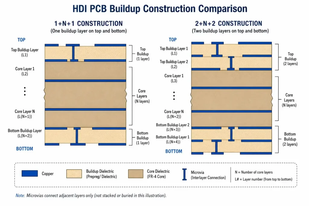
HDI buildup constructions describe how additional routing layers are added to a board core. The “N” represents the number of internal layers in the core. The numbers before and after the “+” indicate how many buildup layers are added to each side of the core. A 1+N+1 board has one buildup layer on the top and one on the bottom. A 2+N+2 board has two buildup layers on each side.
What Does 1+N+1 Mean?
A 1+N+1 HDI board consists of:
- N core layers — These are the internal layers built into the board core, typically using conventional manufacturing processes. The core layers may include ground and power planes, signal layers, and buried vias.
- +1 on top — One buildup layer is added to the top surface of the core. This layer is separated from the core by a thin dielectric and connected using microvias.
- +1 on bottom — One buildup layer is added to the bottom surface of the core, mirroring the top construction.
In a 4-layer 1+N+1 board, N=2 (the core has two internal layers), and one buildup layer is added to each side. The total layer count is 4. In an 8-layer 1+N+1 board, N=6 (six internal core layers) plus one buildup layer on each side.
Microvia connectivity in 1+N+1:
- Buildup layers connect to adjacent core layers via microvia
- Buildup layers cannot directly connect to non-adjacent core layers without using through-hole vias or via stacking
- Via stacking (stacking microvias on buried vias) enables connectivity to deeper layers but increases manufacturing complexity
What Does 2+N+2 Mean?
A 2+N+2 HDI board adds two buildup layers to each side of the core:
- N core layers — Same as 1+N+1
- +2 on top — Two buildup layers are added to the top surface. The first buildup layer (B1) sits on the core. The second buildup layer (B2) sits on B1.
- +2 on bottom — Two buildup layers are added to the bottom, mirroring the top construction
The total layer count includes all core layers plus four buildup layers. An 8-layer 2+N+2 board has 4 internal core layers plus 4 buildup layers (2 on each side).
Microvia connectivity in 2+N+2:
- B1 connects to core layers via microvia
- B2 connects to B1 and core layers via microvia
- Any buildup layer can connect to any other buildup layer or core layer through direct or stacked microvias
- With proper via stacking, any-layer HDI construction can achieve connectivity between any two layers
The Difference Between N+1 and N+N Constructions
Some manufacturers and designers refer to constructions like 1+N+1 as N+1 (referring only to the buildup on one side) or use the notation more generically. The key concept is that the numbers indicate how many thin dielectric layers and microvia stacks are added to each side of the core.
A true any-layer HDI board (sometimes called any-layer or every-layer HDI) allows any layer to connect to any other layer through stacked microvias. This is achievable with 2+N+2 construction and above, and is standard in flagship smartphones.
Quick Verdict: For most applications, choose 1+N+1 HDI for lower cost and simpler manufacturing. Choose 2+N+2 HDI only when routing density, any-layer connectivity, or flagship-level miniaturization justifies the 30–80% cost premium.
Routing Density Comparison
The primary reason to choose 2+N+2 over 1+N+1 is routing density. Each additional buildup layer provides new routing channels that can accommodate fine-pitch traces and high-density fan-out from area-array packages.
1+N+1 Routing Capacity
In a 1+N+1 board, the two outer buildup layers provide routing capacity for component fan-out, high-density routing areas, and signal routing. The internal core layers provide power distribution, ground planes, and additional signal routing.
The limitation of 1+N+1 is that microvias cannot span more than one dielectric layer. A microvia on the outer buildup layer can only reach the adjacent core layer or the adjacent buildup layer. Reaching deeper layers requires through-hole vias or stacked microvia chains.
For a typical design, 1+N+1 works well when:
- The component density is moderate, with few BGAs requiring dense fan-out
- Most signals can be routed on core layers without excessive layer changes
- Via stacking is minimal (microvias go no more than one layer deep)
- The design does not require any-layer connectivity
2+N+2 Routing Capacity
The two buildup layers on each side of a 2+N+2 board provide significantly more routing flexibility. The inner buildup layer (B1) can connect to core layers and to the outer buildup layer (B2). B2 provides the highest routing density for fine-pitch components and critical signals.
2+N+2 enables more complex via stacking strategies:
- Direct microvia from B2 to core (skipping B1) in some designs
- Stacked microvia from B2 to B1 to core for deeper layer access
- Buried via chains that connect multiple internal layers
The additional layers allow designers to route signals on B1 and B2 independently, reducing congestion and enabling more efficient routing.
Manufacturing Complexity and Cost
1+N+1 Manufacturing
1+N+1 HDI is the simpler construction to manufacture:
- One lamination cycle for the core (N core layers)
- One buildup lamination cycle adds the two outer buildup layers
- Microvia formation on one dielectric thickness per side
- Standard registration tolerance between buildup and core layers
The process flow is:
- Build core layers with buried vias (if any)
- Press buildup prepreg and outer layers onto core
- Laser drill microvias in buildup dielectric
- Plate and fill microvias
- Pattern outer buildup layers
1+N+1 is considered the entry point for HDI technology and is widely available from HDI-capable manufacturers.
2+N+2 Manufacturing
2+N+2 is more complex to manufacture:
- Two lamination cycles for the buildup layers (or three for any-layer constructions)
- Two microvia formations per side (one for B1-to-core, one for B2-to-B1)
- Tighter registration between B1 and B2 buildup layers
- Via stacking requires precise alignment across multiple lamination cycles
The process flow is:
- Build core layers with buried vias (if any)
- Press first buildup layer (B1) and its copper
- Laser drill B1 microvias to core
- Plate and fill B1 microvias
- Press second buildup layer (B2) and its copper
- Laser drill B2 microvias to B1 and core
- Plate and fill B2 microvias
- Pattern B1 and B2 layers
Each additional buildup layer adds manufacturing steps, cycle time, and cost. The cumulative registration tolerance across multiple buildup layers must be tightly controlled.
Cost Comparison
| Factor | 1+N+1 | 2+N+2 | Impact |
|---|---|---|---|
| Layer count (example: 6 total) | 4 core + 2 buildup | 2 core + 4 buildup | 2+N+2 has fewer core layers but more buildup |
| Manufacturing cycles | 2 lamination cycles | 3+ lamination cycles | More cycles = higher cost and risk |
| Microvia count | Fewer microvia levels | More microvia levels | More microvias = higher processing cost |
| Registration tolerance | Standard HDI | Tight HDI | Stricter tolerance = lower yield potential |
| Material cost | Standard HDI prepreg | Buildup film + HDI prepreg | Buildup layers use specialty materials |
| Relative cost | Baseline (1.0×) | 1.3–1.8× | Depends on layer count and complexity |
For a board with the same total layer count, 2+N+2 typically costs 30–80% more than 1+N+1 due to additional lamination cycles, more microvia processing, and tighter tolerances.
Electrical Performance Differences
Signal Integrity
2+N+2 boards can offer improved signal integrity in some scenarios because critical signals can be routed on the outermost buildup layers, which have the thinnest dielectrics and shortest interconnect lengths. The additional routing layers also allow for more efficient ground plane placement adjacent to signal layers.
However, the electrical benefit depends on the specific design, not simply the construction type. Both constructions can achieve excellent signal integrity when properly designed.
Power Distribution
Both constructions support power distribution through dedicated planes in the core. The additional buildup layers in 2+N+2 provide flexibility for routing power traces and decoupling capacitor connections, which can improve PDN performance in high-speed designs.
Thermal Performance
Thermal performance is primarily a function of material selection, copper distribution, and board size, not the HDI construction type. Both 1+N+1 and 2+N+2 can be designed for good thermal management when the laminate, copper weights, and thermal vias are properly specified.
Design Guidelines for Each Construction
When to Choose 1+N+1
Choose 1+N+1 HDI when:
- Routing density requirements can be met with the available layers
- The design does not require any-layer connectivity
- Component fan-out can be achieved through standard microvia strategies
- Cost sensitivity is high and 2+N+2 is not justified
- The manufacturer has proven 1+N+1 capability and process control
1+N+1 is the appropriate choice for the majority of HDI applications, including smartphones, tablets, IoT devices, and medical electronics that do not require flagship-level component density.
When to Choose 2+N+2
Choose 2+N+2 HDI when:
- Routing density exceeds what 1+N+1 can provide
- The design requires any-layer connectivity
- High I/O count BGAs require dense multi-layer fan-out
- The board size is constrained and maximum routing efficiency is needed
- The product justifies the cost premium for premium features
2+N+2 is standard in flagship smartphones, advanced networking equipment, high-performance computing, and applications where miniaturization drives competitive advantage.
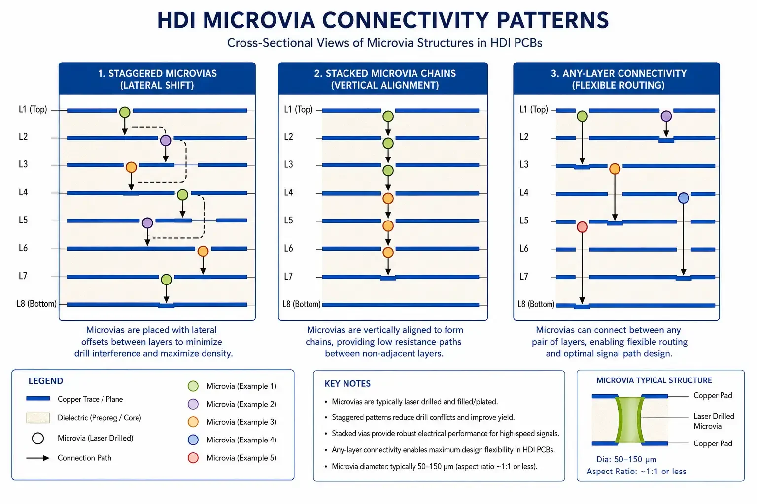
Via Stacking Strategies
Both 1+N+1 and 2+N+2 support via stacking, but the complexity and feasibility differ.
Via Stacking in 1+N+1
In 1+N+1, a microvia on the outer layer can stack on a buried via in the core to reach deeper layers. This is limited by the number of available layers and the aspect ratio of the microvia. Typically, one or two levels of via stacking are feasible.
Example: A microvia from the outer buildup layer stacks on a buried via that connects to an internal core layer.
Via Stacking in 2+N+2
The additional buildup layers in 2+N+2 enable more complex via stacking chains:
- B2 → B1 → Core (two-level stack)
- B2 → Core (direct, skipping B1)
- Stacked combinations for deeper layer access
With careful layer stack design, 2+N+2 can achieve any-layer connectivity where any layer can reach any other layer through appropriate microvia chains.
Via-in-Pad Considerations
Via-in-pad (VIP) construction, where microvias are placed directly in component pad areas, is more common in 2+N+2 designs because the additional buildup layers allow for buried via connections that surface-mount pads can be placed over without exposed vias. VIP requires via filling and capping, which adds cost in both constructions but is more straightforward in 2+N+2.
Material Considerations
Both constructions use similar base materials but may differ in buildup dielectric selection:
Core and inner layer materials are similar for both constructions: standard or high-Tg FR-4, polyimide, or high-frequency laminates depending on the application.
Buildup dielectrics for 1+N+1 typically use laser-drillable prepreg with controlled resin content and flow.
Buildup dielectrics for 2+N+2 may use laser-drillable prepreg, buildup film, or combinations. The second buildup layer (B2) often uses a lower-flow material to prevent voiding over the B1 structures.
Material selection should account for:
- Glass transition temperature (Tg) for lead-free assembly compatibility
- Decomposition temperature (Td) for thermal robustness
- Dielectric constant (Dk) and dissipation factor (Df) for controlled impedance designs
- Coefficient of thermal expansion (CTE) for BGA and via reliability
- Moisture absorption for reflow robustness
Working with Your Manufacturer
Capability Verification
Not all HDI manufacturers can produce 2+N+2 or any-layer HDI. Before specifying a construction, verify that the manufacturer has:
- Laser drilling equipment capable of the required via sizes and densities
- Sequential lamination capability for multiple buildup cycles
- Registration control for multi-layer buildup
- Experience with the specific construction type
- Quality systems for HDI process control
DFM Review
Request a design for manufacturing review from the manufacturer before releasing files. DFM review should cover:
- Minimum line/space capability vs. design values
- Via size, spacing, and annular ring compliance
- Layer stack-up feasibility
- Material availability and alternates
- Test and inspection requirements
Prototype Validation
For complex 2+N+2 designs, a prototype run is recommended to validate:
- Microvia reliability (thermal cycling, pull strength)
- Registration across multiple buildup layers
- Impedance control consistency
- Solder mask and surface finish compatibility
- Assembly yield
Frequently Asked Questions
What is the difference between 1+N+1 and 2+N+2 HDI?
1+N+1 HDI has one buildup layer on each side of the core. 2+N+2 HDI has two buildup layers on each side. The additional buildup layers in 2+N+2 provide higher routing density, more via stacking flexibility, and the potential for any-layer connectivity. The trade-off is higher manufacturing complexity and cost.
Which construction is more cost-effective?
1+N+1 is more cost-effective for most designs. The additional manufacturing cycles and tighter tolerances in 2+N+2 typically add 30–80% to the cost compared to 1+N+1 with equivalent total layer count. Choose 2+N+2 only when the routing density or connectivity requirements justify the premium.
Can 1+N+1 achieve any-layer connectivity?
Standard 1+N+1 cannot achieve full any-layer connectivity because microvias can only span one dielectric layer. With via stacking (microvia stacking on buried via), 1+N+1 can reach deeper layers, but the number of accessible layers and routing flexibility is limited compared to 2+N+2 or any-layer constructions.
What is any-layer HDI?
Any-layer HDI (sometimes called any-layer or every-layer HDI) is a construction where any layer can connect to any other layer through appropriate microvia chains. This is typically achieved with 2+N+2 or higher buildup constructions. Any-layer HDI provides maximum routing flexibility and is used in flagship smartphones.
How do I choose between 1+N+1 and 2+N+2?
Choose based on routing density requirements, any-layer connectivity needs, and budget. If 1+N+1 routing density is sufficient and the design does not require any-layer connectivity, choose 1+N+1 for lower cost and simpler manufacturing. If routing density or any-layer connectivity is required and the budget justifies it, choose 2+N+2.
What are the via size limitations?
Laser-drilled microvia diameters typically range from 80–150 μm (0.003–0.006 inches). Mechanical through-hole vias for layer connectivity range from 150–300 μm or larger. The specific capabilities depend on the manufacturer’s equipment. Discuss via size and aspect ratio requirements with the manufacturer during design.
Does 2+N+2 require different materials than 1+N+1?
Both constructions use similar base materials, but 2+N+2 may require buildup films or specialty laser-drillable prepregs for the second buildup layer. The material selection depends on the manufacturer’s process and the specific design requirements. Confirm material availability with the manufacturer early in the design process.
Final Verdict
The choice between 1+N+1 and 2+N+2 HDI comes down to your specific design requirements and budget constraints.
Choose 1+N+1 HDI if:
- Your routing density requirements can be met with one buildup layer per side
- Cost sensitivity is a primary concern
- Any-layer connectivity is not required
- Your manufacturer has proven 1+N+1 capability
Choose 2+N+2 HDI if:
- Your design requires higher routing density than 1+N+1 can provide
- Any-layer connectivity is specified for the product
- High I/O count BGAs need dense multi-layer fan-out
- The board size is constrained and maximum efficiency is essential
- The application justifies the cost premium (smartphones, networking, HPC)
For a 4–6 layer board with moderate component density, 1+N+1 is almost always the right choice. For 8+ layer boards with flagship-level miniaturization requirements, 2+N+2 provides the routing flexibility and connectivity options that justify the additional manufacturing cost and complexity.
Ready to discuss your HDI requirements? Contact CtrlCPCB for a DFM review and quote on your next HDI project.
References
- Global Electronics Association — IPC standards for HDI and advanced PCB technology.
- JEDEC — Standards for semiconductor packaging and interconnect.
- IEEE — Electronics and interconnect standards.
- SMTA — Electronics manufacturing technical resources.
Further Reading
- HDI PCB Cost — Understanding the cost drivers for HDI manufacturing.
- PCB Stack-Up Design — Designing effective layer stacks.
- Stacked vs Staggered Microvias — Via stacking strategies in HDI.
- Via in Pad Filled and Capped — Manufacturing filled microvias.
- BGA Escape Routing HDI — Fan-out strategies for area-array packages.
- Custom PCB Manufacturer — Working with HDI specialists.
Shanghai Huangte Technology Co., Ltd. | Author: Mike Huang | Published: 2026-07-27
This article provides general engineering guidance for HDI buildup construction selection. Specific design choices should be validated with your HDI manufacturer and evaluated against product requirements for routing density, cost, and performance.