Understanding Gold-Based Surface Finishes
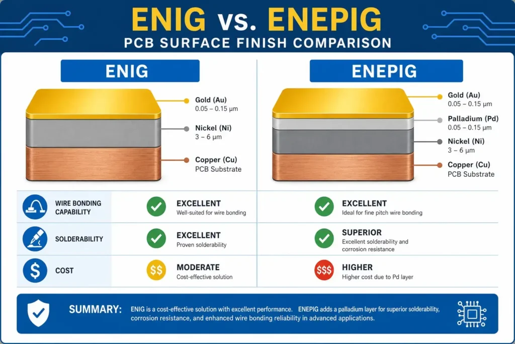
Gold-based surface finishes have become the preferred choice for high-reliability PCB applications due to their excellent solderability, oxidation resistance, and shelf life. Unlike HASL (Hot Air Solder Leveling), which applies solder directly to pads, gold-based finishes use a thin precious metal layer over a nickel barrier.
The two most common gold-based finishes are:
- ENIG (Electroless Nickel Immersion Gold) — Two-layer finish with nickel barrier and gold protection
- ENEPIG (Electroless Nickel Electroless Palladium Immersion Gold) — Three-layer finish adding palladium between nickel and gold
Both finishes meet RoHS and REACH compliance requirements, making them suitable for lead-free assembly processes.
ENIG: Electroless Nickel Immersion Gold
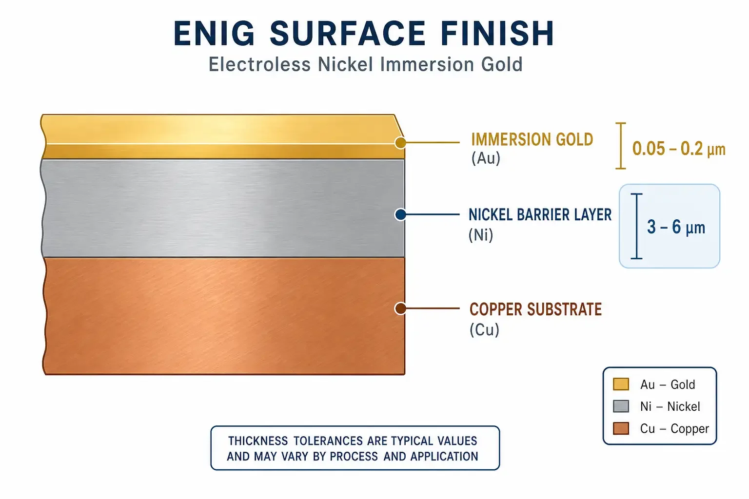
ENIG is a widely adopted surface finish that provides excellent solderability while protecting the underlying copper from oxidation. The electroless nickel layer serves as both a barrier to prevent copper migration and a surface that readily accepts solder. The thin immersion gold layer protects the nickel during storage and dissolves quickly during soldering to expose the nickel surface.
ENIG Process
The ENIG process involves two sequential chemical baths:
- Electroless Nickel Plating — The board is immersed in a nickel solution containing hypophosphite as the reducing agent. Nickel deposits autocatalytically on the catalytic copper surface at approximately 85-90°C. Typical thickness: 3-6 μm.
- Immersion Gold Plating — The nickel-plated board is immersed in a mild gold solution at 80-90°C. Gold deposits by displacement reaction with nickel, replacing surface nickel atoms with gold until a thin, uniform layer forms (0.05-0.2 μm).
ENIG Properties
| Property | Specification | Standard |
|---|---|---|
| Nickel Thickness | 3-6 μm | IPC-4552 |
| Gold Thickness | 0.05-0.2 μm | IPC-4552 |
| Shelf Life | 12 months | Industry standard |
| Surface Flatness | Excellent | – |
| Solderability | Excellent | – |
| Wire Bonding | Gold wire only | Limited |
| Cost Index | 1.5-2.0x vs HASL | Baseline |
ENIG Advantages
ENIG provides excellent solderability and wetting, highly flat surface ideal for fine-pitch components (0.3mm pitch and below), no lead content (RoHS compliant), 12-month shelf life, consistent thickness across the board, and no thermal shock like HASL.
ENIG Limitations
ENIG has higher cost than HASL or OSP, potential “Black pad” syndrome with process variations, limited to gold wire bonding only, aluminum wire bonding not reliable, and cannot withstand multiple reflow cycles indefinitely.
ENEPIG: Electroless Nickel Electroless Palladium Immersion Gold
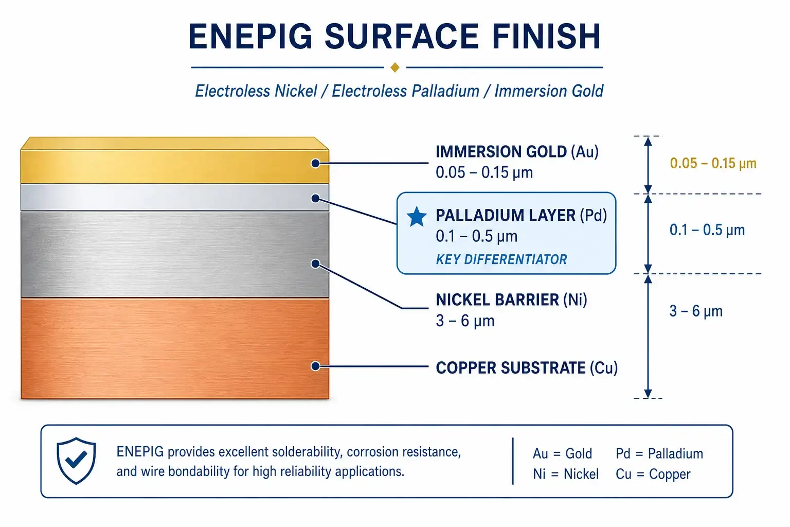
ENEPIG builds on ENIG by adding an electroless palladium layer between nickel and gold. This seemingly simple addition dramatically changes the finish’s capabilities, enabling both solderability and wire bonding while providing superior corrosion resistance.
ENEPIG Process
The ENEPIG process adds a third plating step:
- Electroless Nickel Plating — Same as ENIG, depositing 3-6 μm of nickel at 85-90°C.
- Electroless Palladium Plating — The nickel-plated board is immersed in a palladium solution. Palladium deposits autocatalytically on the nickel surface, forming a uniform layer of 0.1-0.5 μm thickness.
- Immersion Gold Plating — Same as ENIG, a thin gold layer (0.05-0.15 μm) protects the palladium and provides the characteristic gold appearance.
ENEPIG Properties
| Property | Specification | Standard |
|---|---|---|
| Nickel Thickness | 3-6 μm | IPC-4554 |
| Palladium Thickness | 0.1-0.5 μm | IPC-4554 |
| Gold Thickness | 0.05-0.15 μm | IPC-4554 |
| Shelf Life | 12+ months | Industry standard |
| Surface Flatness | Excellent | – |
| Solderability | Excellent | – |
| Wire Bonding | Gold and aluminum | Full support |
| Cost Index | 2.0-3.0x vs HASL | Premium |
ENEPIG Advantages
ENEPIG enables aluminum wire bonding (20-25 μm diameter typical), provides superior corrosion resistance, prevents nickel diffusion (black pad resistance), withstands multiple reflow cycles (5+ passes), suits both solder assembly and wire bonding, excels for HDI and fine-pitch applications, and offers extended shelf life vs ENIG.
ENEPIG Limitations
ENEPIG has the highest cost among common finishes, requires more complex process control, needs longer processing time, and demands specialized equipment.
Layer-by-Layer Comparison
Understanding each layer’s purpose clarifies why ENEPIG outperforms ENIG for certain applications.
Gold Layer (Both Finishes)
The gold layer serves primarily as a protective coating during storage. At only 0.05-0.2 μm thickness, gold dissolves within seconds during soldering, exposing the underlying layer. Gold provides oxidation resistance during storage, immediate solderability after gold removal, and cosmetic appearance.
Nickel Layer (Both Finishes)
Nickel serves dual functions as both a barrier and solderable surface. As barrier function, it prevents copper diffusion into solder joints. For solderability, it provides excellent wetting for SnAgCu and other lead-free alloys. Nickel provides mechanical support and gives the finish mechanical integrity. Nickle is the workhorse layer providing the actual solderability; the gold layer merely protects it until soldering.
Palladium Layer (ENEPIG Only)
Palladium is the key differentiator that enables ENEPIG’s enhanced capabilities. It prevents nickel diffusion, stops nickel atoms from migrating into the gold layer, protects against “black pad,” eliminates the primary failure mode of ENIG, enables aluminum wire bonding, provides metallurgically compatible surface for thermosonic bonding, and enhances corrosion resistance by adding another barrier against environmental factors.
ENIG vs ENEPIG: Key Differences
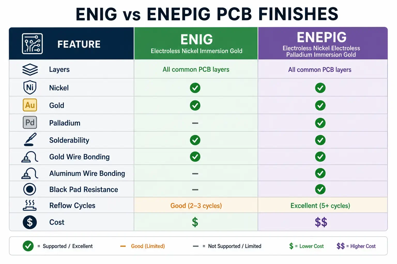
| Parameter | ENIG | ENEPIG |
|---|---|---|
| Layers | Nickel + Gold | Nickel + Palladium + Gold |
| Nickel Thickness | 3-6 μm | 3-6 μm |
| Palladium Thickness | None | 0.1-0.5 μm |
| Gold Thickness | 0.05-0.2 μm | 0.05-0.15 μm |
| Solderability | Excellent | Excellent |
| Gold Wire Bonding | Yes | Yes |
| Aluminum Wire Bonding | No | Yes |
| Black Pad Resistance | Moderate | Excellent |
| Reflow Cycles | 3-5 | 5+ |
| Shelf Life | 12 months | 12+ months |
| Surface Flatness | Excellent | Excellent |
| Cost vs HASL | 1.5-2.0x | 2.0-3.0x |
| Cost vs ENIG | Baseline | 1.2-1.5x |
| IPC Standard | IPC-4552 | IPC-4554 |
When to Choose ENIG
Choose ENIG when solderability is the primary requirement (SMT components only, no wire bonding needed), cost-sensitive applications where budget constraints favor lower-cost finishes, standard multilayer boards with conventional assembly and proven yields, consumer electronics where high-volume products where finish cost impacts margins, BGA and fine-pitch components where excellent flatness supports 0.4mm+ pitch devices, and single or dual reflow with limited assembly cycles.
Typical ENIG Applications
- Smartphone PCBs and accessories
- Computer peripherals
- Consumer electronics
- Standard communication equipment
- LED drivers and controllers
- Industrial control boards
When to Choose ENEPIG
Choose ENEPIG when aluminum wire bonding is required (sensors, RF modules, memory devices), dual-purpose assembly where both solder components and wire-bond dies are on same board, enhanced reliability needed for automotive, medical, aerospace applications, multiple reflow cycles where complex assembly with 5+ solder passes is expected, HDI and ultra-fine pitch at 0.3mm pitch and below, black pad concerns where applications where failure is unacceptable, and long product lifecycle with 10+ year reliability requirements.
Typical ENEPIG Applications
- Automotive electronics — ECUs, ADAS modules, safety systems
- Medical devices — Implantable sensors, diagnostic equipment
- RF and microwave modules — Power amplifiers, filters with wire-bonded dies
- Memory modules — DDR, flash storage with wire-bonded NAND dies
- LED modules — High-power LEDs with bonded driver ICs
- Aerospace systems — Avionics with high reliability requirements
Cost Comparison and Value Analysis
Direct Cost Comparison
| Finish | Relative Cost | Use Case |
|---|---|---|
| HASL | 1.0x | Budget, legacy |
| OSP | 1.0-1.2x | Simple boards |
| ENIG | 1.5-2.0x | Premium solderability |
| ENEPIG | 2.0-3.0x | Wire bonding + solderability |
When the Premium is Justified
ENEPIG’s 20-50% premium over ENIG is justified when wire bonding eliminates separate interposer (combined process saves assembly cost), field failure costs are unacceptable (black pad reliability is critical), manufacturing complexity reduced (single finish for all assembly steps), or customer specification mandates ENEPIG (qualification requirements).
IPC Standards Reference
Both ENIG and ENEPIG have dedicated IPC standards defining thickness, process, and quality requirements:
| Standard | Finish | Key Specifications |
|---|---|---|
| IPC-4552 | ENIG | Nickel 3-6 μm, Gold 0.05-0.2 μm |
| IPC-4554 | ENEPIG | Nickel 3-6 μm, Palladium 0.1-0.5 μm, Gold 0.05-0.15 μm |
These standards ensure consistent quality and performance across different manufacturers. When specifying finishes for qualification, always reference the applicable IPC standard.
Frequently Asked Questions
What is the difference between ENIG and ENEPIG?
ENIG (Electroless Nickel Immersion Gold) has two layers: nickel (3-6 μm) for barrier and solderability, with thin gold (0.05-0.2 μm) for protection. ENEPIG adds a palladium layer (0.1-0.5 μm) between nickel and gold. This palladium layer prevents nickel diffusion, enables aluminum wire bonding, and provides superior corrosion resistance. Both finishes offer excellent solderability, but only ENEPIG supports aluminum wire bonding.
When should I choose ENEPIG instead of ENIG?
Choose ENEPIG when aluminum wire bonding is required (such as sensor dies, RF modules, or memory devices), when both solderability and wire bonding are needed on the same board, when enhanced reliability and black pad resistance are critical, or when the board will undergo 5+ reflow cycles. ENEPIG costs 20-50% more but provides capabilities ENIG cannot match.
What is the purpose of each layer in ENIG and ENEPIG?
The gold layer (both finishes) provides oxidation protection during storage and dissolves quickly during soldering to expose nickel. The nickel layer provides the actual solderability and acts as a barrier preventing copper migration. In ENEPIG, the palladium layer prevents nickel diffusion into gold (eliminating black pad issues), enables aluminum wire bonding, and provides an additional corrosion barrier.
What are the IPC thickness specifications?
Per IPC standards: ENIG (IPC-4552) requires nickel 3-6 μm thickness and gold 0.05-0.2 μm. ENEPIG (IPC-4554) requires nickel 3-6 μm, palladium 0.1-0.5 μm, and gold 0.05-0.15 μm. Always specify the IPC standard in your PCB documentation to ensure consistent quality across manufacturers.
Can ENEPIG boards be used for both soldering and wire bonding?
Yes, ENEPIG is specifically designed for dual-use applications. The palladium layer enables reliable aluminum wire bonding (typically 20-25 μm diameter) while the nickel surface provides excellent solderability for SMT components. This makes ENEPIG ideal for modules that combine surface-mount components with wire-bonded dies, such as sensor modules, RF front-ends, and memory devices.
What are the cost implications of choosing ENEPIG?
ENEPIG typically costs 20-50% more than ENIG due to the additional palladium layer and more complex process. For high-volume applications requiring wire bonding, however, ENEPIG may reduce total system cost by eliminating the need for separate wire-bonding substrates or interposers. The premium is typically justified when field reliability is critical, aluminum wire bonding is required, or the application demands enhanced corrosion resistance.
References
- IPC-4552, “Specification for Electroless Nickel/Electroless Palladium/Immersion Gold (ENEPIG) Finish for Printed Boards,” IPC, 2024.
https://www.ipc.org/ - IPC-4554, “Specification for Electroless Nickel/Electroless Palladium/Immersion Gold (ENEPIG) Finish for Printed Boards,” IPC, 2024.
https://www.ipc.org/ - IPC-6012, “Qualification and Performance Specification for Rigid Printed Boards,” IPC, 2024.
https://www.ipc.org/ - SMTA, “Surface Finish Selection Guide,” Surface Mount Technology Association Technical Resources, 2025.
https://www.smta.org/
Further Reading
- Custom PCB Manufacturer — Find a manufacturer for your ENIG or ENEPIG PCB requirements
- PCB Surface Finish Comparison — Overview of all surface finish options
- PCB Quote Requirements — Specify finish requirements in your RFQ
CtrlCPCB | Shanghai Huangte Technology Co., Ltd. | Last updated: 2026-07-23
This article is for informational purposes. Consult with your PCB manufacturer to determine the optimal surface finish for your specific assembly requirements, reliability targets, and cost constraints.