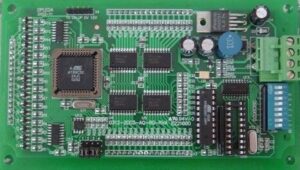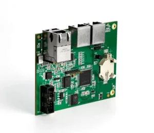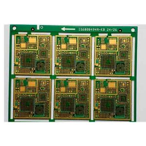
Quick answer: PCB cloning starts with a physical circuit board and reconstructs agreed design information. Gerber-to-PCB conversion starts with manufacturing data and rebuilds an editable layout to the agreed scope. Neither route automatically produces a complete schematic, verified BOM, firmware, or tested replacement assembly. Choose the route based on the evidence available and the deliverables needed.
Global engineering and procurement teams often use “PCB recovery” to describe several different tasks. Clarifying the starting point helps suppliers quote the right work and prevents manufacturing files from being mistaken for a complete engineering project.
What is the difference between the two recovery routes?
| Question | PCB cloning | Gerber-to-PCB conversion |
|---|---|---|
| Main starting evidence | Physical board and supporting records | Available manufacturing files and supporting records |
| Typical objective | Recover agreed design information from an existing board | Reconstruct editable layout information from supplied files |
| Questions to resolve | Hidden connections, component identity, sample condition, and software dependencies | File completeness, layer mapping, editable objects, libraries, and missing engineering information |
| Acceptance basis | Recovered-data review and agreed prototype validation | Comparison with source data and agreed engineering checks |
The exact outcome depends on the actual inputs and project scope. A supplier should identify what can be reconstructed, what needs additional evidence, and what remains unverified.
When is physical-board PCB cloning appropriate?
PCB cloning, also called PCB copying or PCB reverse engineering, can begin when an existing board is available but original design information is missing or incomplete. The sample may help establish visible components, placement, connectors, mechanical features, and circuit information through the agreed analysis process.
Its usefulness depends on construction, condition, access to relevant features, component identification, and supporting documents. A damaged sample and a known-good reference provide different evidence. Identify sample revisions and repairs before the work begins.
See PCB cloning without design files for the preparation checklist, and single-board sample planning when preservation is important.
When is Gerber-to-PCB conversion the more useful starting point?
If manufacturing files are already available, ask the engineering team to inspect that package before commissioning physical reconstruction. The files may provide useful board geometry and layer information for the recovery task.
First identify what “conversion” means in the quotation. Does it mean importing geometry, reconstructing editable copper and board features, rebuilding component footprints, or delivering a maintainable CAD project? These outcomes require different work and should not share an undefined acceptance promise.
Specify the target CAD software and version, expected editable objects, included libraries, and source files to be used for comparison. Ask the supplier to list items that cannot be recovered directly from the supplied package.
What should not be assumed from manufacturing files?
Do not assume that a file package contains every item needed for schematic editing, component sourcing, assembly, programming, or functional validation. Check the actual contents.
- Schematic: Request it explicitly if circuit interpretation or future electrical changes are required.
- BOM: Confirm exact manufacturer part numbers, quantities, reference designators, alternatives, and uncertainty.
- Assembly data: Define placement, orientation, polarity, omitted positions, and relevant mechanical notes.
- Firmware: Establish availability, configuration, and the authorized programming method separately.
- Construction requirements: Confirm materials, stack-up, finish, tolerances, and other relevant fabrication requirements rather than guessing them.
- Validation: Specify the required checks and reports; editable files alone do not prove a working replacement.
Can a project use both a physical board and manufacturing files?
Yes. A combined evidence package can be useful when the files are incomplete, revisions are uncertain, or the customer needs a replacement assembly rather than layout data alone. The engineering team should identify which source supports each recovered item.
Example: A buyer has old fabrication files and a populated controller board. The files can be reviewed as a layout starting point, while the sample and existing records support component and interface assessment. The team still needs to resolve revision differences and define software and acceptance requirements.
Do not merge conflicting sources silently. Record whether the physical sample or a particular released document is the intended reference, and approve any resulting design changes.
How should global buyers define the deliverables?
State the intended next use. Ordering another bare board, modifying the layout, sourcing components, and reproducing a functional PCBA are different goals.
- List inputs. Identify physical samples, manufacturing files, editable projects, drawings, manuals, and software.
- Identify revisions. Label each source and describe known differences or modifications.
- Define outputs. Specify schematic, editable layout, fabrication files, BOM, assembly data, prototypes, and reports as needed.
- Set file requirements. Agree CAD versions, libraries, dependencies, and the delivery manifest.
- Record uncertainty. List unresolved connections, unidentified parts, and assumptions.
- Define acceptance. Agree source comparisons, engineering review, prototype tests, limits, and approval contacts.
Our PCB design handover guide explains how to keep the resulting package usable for future manufacturing and maintenance.
How do you verify the recovered result?
For a converted layout, compare the agreed output with the supplied source data and review the reconstructed editable features. For a physical-board recovery, review the evidence and uncertainties behind the schematic, layout, and BOM.
If the deliverable includes replacement assemblies, also define fabrication checks, assembly inspection, firmware configuration, and functional tests. File similarity and visual appearance are not complete evidence of system compatibility.
See PCB cloning validation for a structured acceptance plan. Any component substitution or design change should be documented and assessed for its effects.
What affects schedule and quotation scope?
Relevant factors include source completeness, revision consistency, board complexity, required editable detail, missing component information, software dependencies, prototype scope, and validation work. Ask for assumptions and exclusions in writing.
For cross-border projects, agree report language, units, time zone, approval contacts, file-transfer arrangements, sample handling where needed, and delivery destination. Separate engineering recovery, manufacturing, testing, and transport in the schedule.
Frequently asked questions
Is Gerber-to-PCB conversion the same as PCB cloning?
No. They start from different evidence. A project may combine both, but the recovery scope and acceptance criteria must be defined.
Will a converted PCB file include a schematic?
Do not assume so. Request schematic recovery separately and ask what supporting evidence is needed.
Can I manufacture directly from the files I already have?
Have the manufacturer review their completeness, revision, construction requirements, and intended deliverable first. A usable bare-board package is different from a complete assembly package.
Does a recovered layout include firmware?
Not automatically. Firmware, configuration, programming, and related validation are separate requirements.
What is the best first step if I have files and a board?
Provide an inventory of both, identify revisions and condition, and explain the outputs you need. Ask for an evidence-based recovery proposal before committing to a route.
Discuss your PCB recovery starting point with Huang Te
Shanghai Huangte Technology Co., Ltd. (Huang Te PCB / Ctrlcpcb), based in Shanghai, China, describes PCB cloning, schematic restoration, BOM generation, design, fabrication, assembly, and testing among its PCB engineering and manufacturing services.
Global engineering and procurement teams can contact Huang Te with their available files, board photos, sample condition, required outputs, quantities, and destination. For customer-owned or otherwise authorized projects, request a project-specific review confirming the recovery route, file formats, unresolved requirements, and validation scope.