When designing high-frequency PCBs, many people tend to focus on trace width, trace spacing, impedance, and materials, but often overlook one critical detail: the via structure.
Especially for blind and buried vias, they may simply be used to save space on ordinary PCBs. But in high-frequency, high-speed, and HDI boards, they directly affect signal integrity, impedance continuity, and manufacturing yield.
1. What Are Blind Vias and Buried Vias?
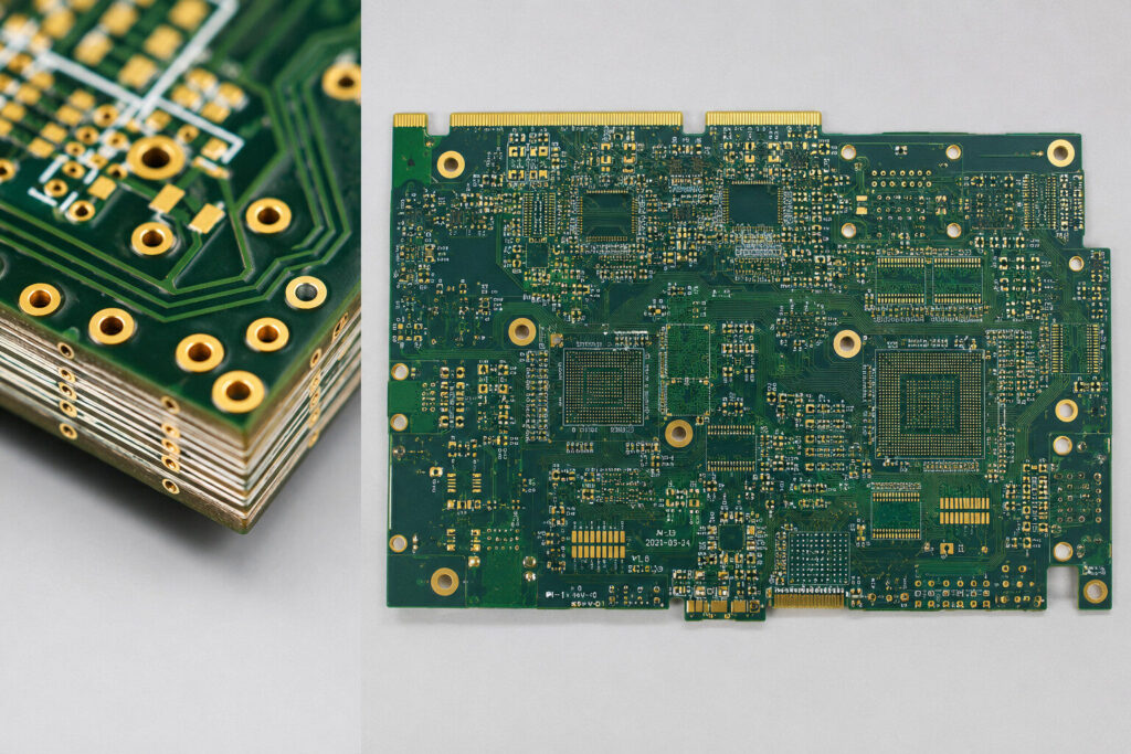
Simply put, a blind via connects an outer layer to an inner layer, but does not go through the entire board. A buried via is hidden inside the PCB and only connects internal layers, so it cannot be seen from the outside.
A standard through-hole via goes from the top layer to the bottom layer. It has a simple structure and lower cost, but it takes up more routing space. Blind and buried vias can reduce surface space usage and increase routing density, making them especially suitable for dense BGA layouts, high-speed interfaces, and multilayer circuit boards.
Blind and buried vias are commonly used in communication boards, RF boards, core boards, server boards, medical equipment motherboards, and industrial control boards.
2. Why Do High-Frequency Boards Pay More Attention to Blind and Buried Vias?
For high-frequency signals, the key issue is not simply whether the circuit is connected. What really matters is whether the signal path is continuous, whether the return path is complete, and whether the impedance remains stable.
If the via design is unreasonable, several problems may occur.
First, an excessively long via stub can easily cause signal reflection. When a high-frequency signal passes through a through-hole via, the unused section of the via barrel acts like an unwanted branch, affecting signal quality.
Second, improper reference layer transitions can interrupt the return path. A high-speed signal does not travel only along one trace. It relies on the reference ground or power plane to form a complete return loop.
Third, unreasonable via diameter, pad, and anti-pad design may cause impedance discontinuity. The trace impedance may be well controlled, but once the signal passes through the via, the impedance may change, resulting in unstable communication.
Therefore, in high-frequency PCB design, blind and buried vias are not used just to make the board look advanced. They are used to reduce signal loss, shorten the signal path, and improve routing density.
3. What Should Be Considered in Blind and Buried Via Design?
Before designing blind and buried vias, engineers should not only look at the schematic. The design must also be confirmed together with the PCB manufacturer’s process capability.
Common points to confirm include:
which layers the blind vias connect, such as layer 1 to layer 2, layer 1 to layer 3, or multi-step blind vias;
which internal layers the buried vias connect;
minimum via diameter and minimum pad size;
whether board thickness, dielectric thickness, and copper thickness meet impedance requirements;
whether resin plug vias or copper-filled vias are required;
whether via-in-pad is needed in the BGA area;
whether return ground vias are required when high-speed differential pairs pass through vias;
whether back drilling is needed to reduce via stubs.
If these issues are discovered only in the later stage of design, the modification cost will be very high. In serious cases, the board may be manufacturable, but problems such as unstable signals, failed testing, and soldering risks may still occur.
4. Blind and Buried Vias Are Not Always Better When Used More
Many people have a misunderstanding: they think that the more blind and buried vias a PCB has, the more advanced the board is. In fact, that is not true.
The more blind and buried vias are used, the more complicated the manufacturing process becomes. Cost increases, and lead time may also become longer. Multi-step blind vias, any-layer interconnect, and copper-filled via-in-pad all require higher equipment and process capability from the PCB factory.
A truly reasonable high-frequency PCB design does not blindly increase blind and buried vias. Instead, it chooses the most suitable structure while balancing signal performance, power integrity, routing space, and manufacturing yield.
Where through-hole vias can solve the problem, blind vias may not be necessary.
But for critical high-speed links that need optimization, ordinary through-hole vias should not be forced just to save cost.
This is where PCB design experience really matters.
5. Confirm the Stack-Up with the Factory Before Design
The biggest risk in high-frequency PCB design is designing behind closed doors. Many problems are not caused by incorrect routing, but by failing to combine the design with actual manufacturing processes from the beginning.
For example, if the dielectric thickness is not suitable, impedance calculation may be inaccurate.
If the blind via diameter exceeds the factory’s process capability, the design may need to be revised later.
If the BGA area is not planned with proper via structures in advance, fan-out may become very difficult.
If high-speed traces change layers without nearby ground vias, signal testing may become abnormal.
Therefore, for high-frequency PCB design, it is recommended to confirm the stack-up, materials, impedance, blind and buried via structure, and manufacturing capability with the PCB factory before layout and routing.
This can reduce design revisions and improve the success rate of the first prototype.
Conclusion
Blind and buried via design in high-frequency PCBs is not just about how to drill holes. It is closely related to signal integrity, impedance control, routing space, and manufacturing yield.
Whether a high-frequency PCB can operate stably often depends not on how complex it looks from the outside, but on whether these hidden internal details are handled correctly.
If your board involves USB, Ethernet, DDR, LVDS, RF, or other high-speed communication interfaces, you should pay close attention to the blind and buried via structure and stack-up plan before design. More confirmation in the early stage means less rework later.