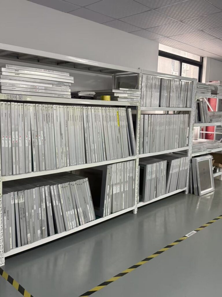
In SMT assembly, many people focus on pick-and-place machine accuracy, reflow soldering temperature, and AOI inspection, but they often overlook one very important process — stencil technology.
In fact, solder paste printing is the first core process in SMT production. The stencil is the key tool that determines whether solder paste can be accurately deposited onto the PCB pads. Whether the stencil apertures are properly designed, whether the thickness is suitable, and whether the stencil tension is stable will directly affect the final soldering quality.
1. What Is the Function of a Stencil?
A stencil is mainly used for solder paste printing. During production, solder paste is printed onto the PCB pads through the stencil apertures under the pressure of a squeegee. After that, the components are mounted and soldered through the reflow process.
Simply put, the stencil’s job is to apply solder paste to the pads in a fixed position, controlled amount, and stable manner.
If there is too little solder paste, issues such as insufficient solder or cold solder joints may occur.
If there is too much solder paste, problems such as solder bridging, solder balls, or short circuits may happen.
If the solder paste position is misaligned, even a high-precision pick-and-place machine may not be able to fully compensate for it.
So although a stencil may look like just a thin stainless steel sheet, it directly affects the soldering yield of the entire PCBA batch.
2. What Are the Common Stencil Processes?
Common stencil processes include laser-cut stencils, chemically etched stencils, and electroformed stencils. Among them, laser-cut stencils are the most commonly used in SMT production.
Laser-cut stencils use high-precision laser cutting to create apertures. The aperture walls are relatively straight, and the dimensional consistency is good, making them suitable for most SMT assembly projects. For precision components such as 0402, 0201, BGA, and QFN, stencil aperture accuracy is even more critical. Processes such as electropolishing and nano-coating are often used to reduce solder paste adhesion on the aperture walls and improve paste release.
For high-density PCBs, fine-pitch ICs, or BGA components, stencil aperture design cannot simply copy the pad size. It must be adjusted based on the component package, pad size, spacing, solder paste type, PCB thickness, and process capability.
3. How Should Stencil Thickness Be Selected?
Stencil thickness is not simply “the thicker, the better,” nor is it “the thinner, the better.”
Common SMT stencil thicknesses are usually around 0.10 mm, 0.12 mm, 0.13 mm, and 0.15 mm. The thicker the stencil, the more solder paste is deposited. The thinner the stencil, the less solder paste is deposited.
For standard SMD components, a conventional stencil thickness is usually sufficient.
For fine-pitch ICs, QFN, BGA, and similar components, an overly thick stencil may easily cause solder bridging.
For high-power components, connectors, shielding covers, and large pads, a stencil that is too thin may result in insufficient solder volume.
Therefore, for more complex PCB projects, step stencils may be used. Areas that require more solder paste can be locally thickened, while areas that require less solder paste can be locally reduced, ensuring that different components receive the proper solder paste volume.
4. Why Does Stencil Aperture Design Need Optimization?
Many soldering defects are not caused by the pick-and-place machine. Instead, the hidden risks often begin during stencil aperture design.
For example, if the large thermal pad in the center of a QFN package is fully opened, too much solder paste may be deposited. After reflow, this can cause the component to float or create voids. In this case, a segmented aperture design is usually used to control the solder paste release volume.
For fine-pitch ICs, if the stencil apertures are opened exactly according to the pad size, excessive solder paste may easily lead to bridging. The aperture width may need to be reduced, or an anti-bridging design may be applied.
For BGA pads, the focus is more on stable solder paste release and aperture wall quality. Aperture roundness, wall smoothness, and stencil tension can all affect solder paste formation.
Therefore, stencil design is not simply “opening holes according to the pads.” It must be optimized according to the actual soldering process.
5. How Does Stencil Technology Affect PCBA Quality?
When stencil technology is well controlled, solder paste printing becomes more uniform, and the stability of component placement and reflow soldering also improves.
When stencil technology is not properly controlled, problems such as solder bridging, cold solder joints, component misalignment, solder balls, open solder joints, and tombstoning may occur later in production.
This is especially important when moving from small-batch prototyping to mass production. If a sample can be soldered successfully, it does not necessarily mean that mass production will be stable. Mass production places higher demands on stencil design, printing parameters, reflow profiles, and inspection processes.
A qualified PCBA is not only about accurate component placement. It also depends on careful control of every step, including stencil design, solder paste, printing, reflow soldering, and AOI inspection.
Conclusion
Although a stencil is only one tool in SMT production, it serves as the first quality control point for soldering. For high-density, high-precision, and high-reliability circuit boards, stencil design and process control are extremely important.
Stable PCBA production is not only about having advanced equipment. It also depends on whether every process detail is treated seriously.