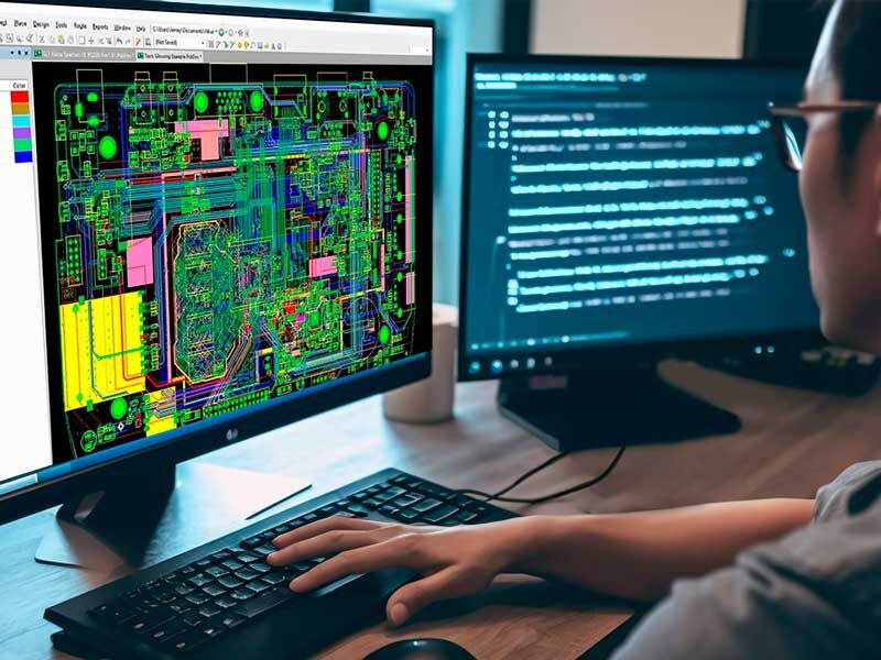
A Printed Circuit Board (PCB) is not only the physical carrier of electronic components but also the core bridge for signal and power transmission. While many users focus on PCB layer count and size, the manufacturing process, material selection, and reliability control directly determine whether electronic products can operate stably in long-term, high-temperature, high-frequency, and complex electromagnetic environments. For industrial electronics, automotive devices, and communication equipment, PCB process quality is the bottom line of product safety and durability.
1. Overview of Standard PCB Manufacturing Process
The production of high-quality PCBs involves dozens of precision processes from raw material input to finished product delivery. Each procedure has strict technical standards to avoid open circuits, short circuits, delamination, and signal attenuation.
Material Cutting and Inner Layer Processing: The whole copper-clad laminate is cut according to product specifications. The inner circuit pattern is transferred through exposure and development, and redundant copper foil is etched to form complete inner conductive circuits. This step is critical for multilayer PCBs, laying the foundation for subsequent lamination and conduction.
Layer Alignment and Lamination: For double-sided and multilayer boards, insulating prepreg and copper layers are stacked in strict accordance with design requirements. High temperature and high pressure are applied for lamination to ensure tight bonding between layers, preventing layer separation and air voids that may cause circuit failure.
Drilling and Metallization: Precision drilling machines create via holes, component holes, and positioning holes on the laminated board. The hole wall is plated with copper through chemical copper deposition and electroplating processes to realize electrical conduction between different layers, which is the key to multi-layer signal interconnection.
Outer Circuit Etching and Solder Mask Printing: The outer layer circuit is formed by the same exposure and etching technology. After surface cleaning, a solder mask ink is coated and cured to protect the circuit. Finally, silkscreen printing is completed to mark component positions and parameters.
Surface Finishing and Quality Testing: Common surface treatment processes include HASL, ENIG, OSP, and silver plating, which improve solderability and oxidation resistance of the PCB. After production, strict electrical testing, impedance testing, and appearance inspection are carried out to eliminate defective boards.
2. Common PCB Surface Finishing Technologies and Their Advantages
Surface finishing is a key process to ensure PCB welding performance and anti-oxidation capability. Different processes are selected according to product application scenarios:
OSP (Organic Solderability Preservative): It forms an organic protective film on the copper surface. With low cost and flat surface, it is suitable for ordinary consumer electronic products and mass production. It features excellent solderability and meets the welding requirements of conventional SMT processes.
ENIG (Electroless Nickel Immersion Gold): Also known as gold plating, it provides ultra-flat surface, strong oxidation resistance, and excellent conductivity. It is widely used in high-precision products such as 5G communication boards, medical equipment, and automotive electronic core boards, and is very suitable for fine-pitch component welding.
HASL (Hot Air Solder Leveling): A traditional and mature process with good welding reliability and low cost. It is mostly used in industrial control equipment and household appliances with ordinary precision requirements.
3. Core Factors Affecting PCB Reliability
Poor PCB reliability will lead to common failures such as device crash, signal distortion, circuit short circuit, and board burnout in terminal equipment. The main influencing factors are summarized as follows:
Material Quality: Substrate Tg value, thermal expansion coefficient, and copper foil thickness determine the high-temperature resistance and structural stability of the PCB. Inferior substrates are prone to deformation and delamination when heated, resulting in circuit damage.
Process Precision: Inaccurate line width and spacing, incomplete hole metallization, and insufficient lamination pressure will cause hidden dangers such as high impedance, poor conduction, and easy short circuit of the circuit.
Environmental Adaptability: Humidity, high temperature, and electromagnetic interference in the working environment will affect the service life of the PCB. Professional anti-interference design and environmental protection processes can effectively improve the product’s weather resistance.
4. The Importance of Strict PCB Quality Control
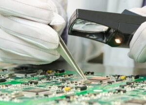
In the electronic manufacturing industry, PCB quality determines the overall yield and after-sales stability of terminal products. Strict quality control runs through the entire production process: raw material incoming inspection, first-piece confirmation in each process, random inspection of semi-finished products, and full inspection of finished products. Professional manufacturers adopt automated optical inspection (AOI), flying probe testing, and impedance testing to ensure that each PCB meets design standards.
Stable PCB process and reliable quality control can effectively reduce product failure rates, lower after-sales maintenance costs, and help terminal brands improve market credibility and product competitiveness.
Conclusion
PCB manufacturing is a highly systematic and precise engineering technology. Simple board making cannot meet the needs of modern high-end electronic equipment. Only by relying on standardized production processes, high-quality raw materials, and strict quality inspection systems can we produce high-reliability PCBs that adapt to complex working conditions. As electronic products continue to develop toward high frequency, high speed, and miniaturization, fine process control and high-reliability manufacturing will become the core competitiveness of the PCB industry.