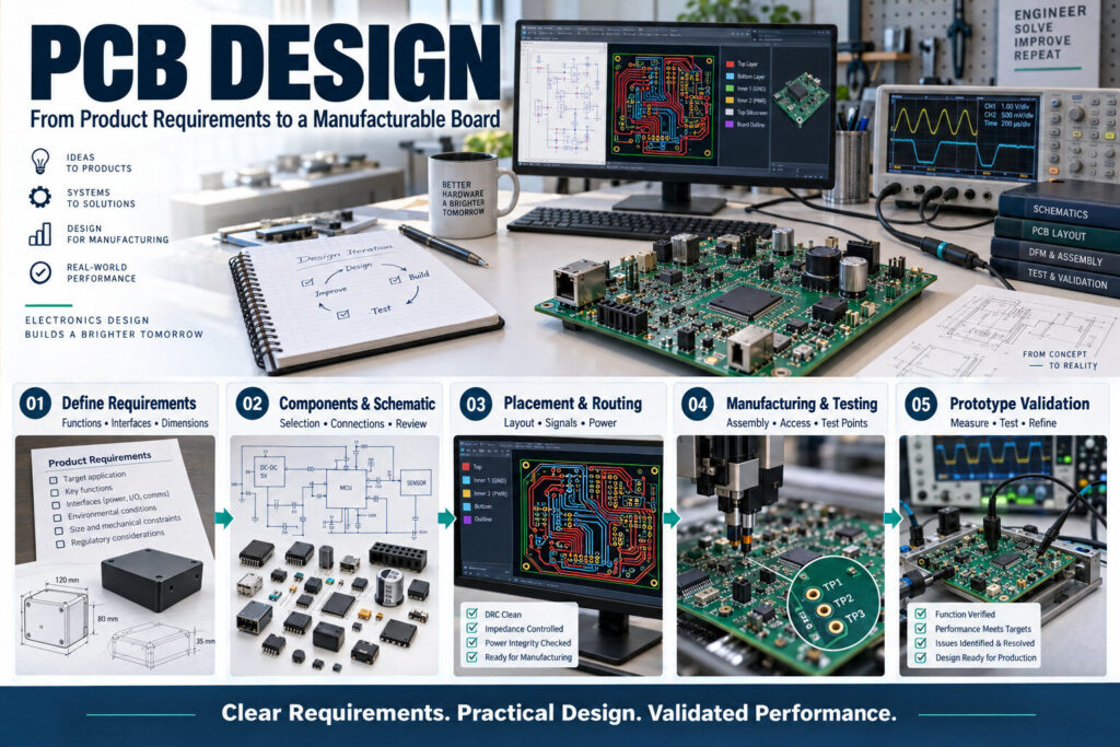
PCB design begins before the first trace is drawn. A useful design must translate product requirements into a circuit that fits the enclosure, supports the required functions, and can be manufactured and tested.
Define the Product Requirements
The first step is to describe what the product must do. Important details include the power source, interfaces, board dimensions, installation method, operating environment, and expected production volume.
Requirements should be specific enough to verify. For example, “supports communication” is less useful than identifying the interface, connected equipment, and required operating conditions.
Select Components and Develop the Schematic
Component selection balances technical performance, availability, cost, and long-term support. Key devices should be evaluated together with their supporting circuits.
The schematic records how the circuit works and how components connect. Reviewing power connections, signal interfaces, protection circuits, and programming connections at this stage can prevent avoidable problems later.
Plan Placement and Routing
Board layout turns the schematic into a physical arrangement. Connector locations, mounting holes, enclosure clearances, and heat-generating components often influence placement early in the process.
Routing must account for the needs of different circuits. Power paths, sensitive analog signals, and fast digital interfaces may require different treatment. A board that passes basic design-rule checks still needs engineering review.
Consider Manufacturing and Testing
A design should be practical to assemble and inspect. Component spacing, soldering access, clear markings, and suitable test points can make production and troubleshooting easier.
Manufacturing requirements should be discussed with the intended supplier. Available processes and capabilities may influence the board structure and layout.
Build and Validate a Prototype
The first prototype provides evidence that the design works as intended. Verification may include electrical measurements, firmware checks, mechanical fit, thermal behavior, and operation with the actual equipment.
Problems found during testing should be documented, corrected, and checked again. Any changes should be reflected in the schematic, PCB files, and bill of materials.
A completed layout is an important milestone, but it is not the end of product development. A strong PCB design is supported by clear requirements, coordinated documentation, and test results that demonstrate its suitability for use.