PCB design is both an electrical task and a manufacturing task. A board must connect components correctly, but it must also be practical to fabricate, assemble, inspect, and repair. Considering these requirements early can prevent costly changes later.
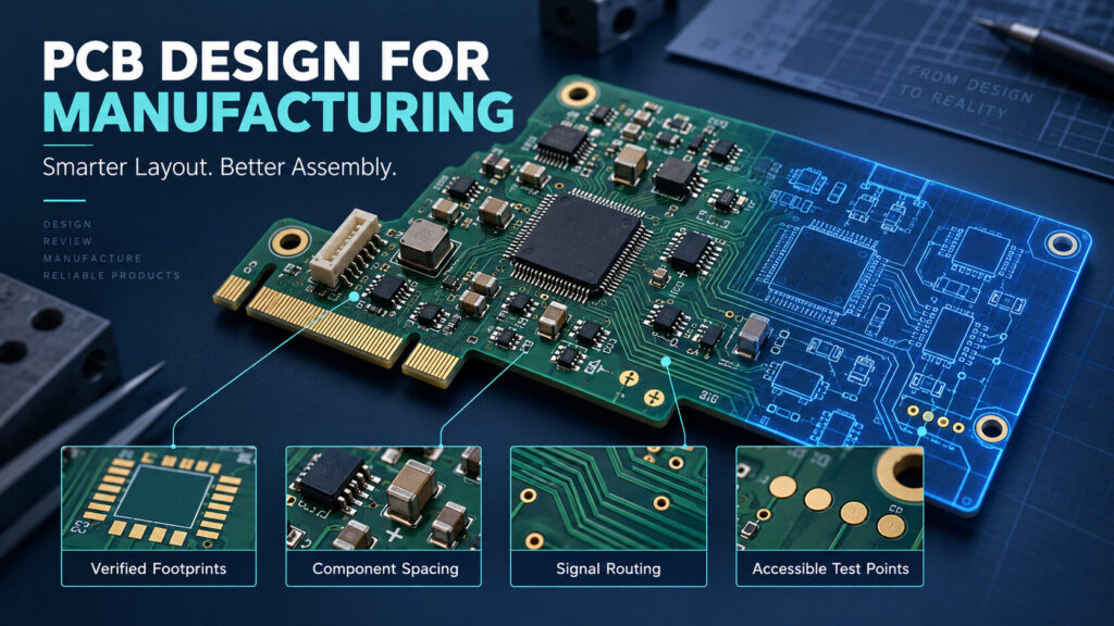
The process begins with a clear schematic and verified component footprints. Each footprint should match the intended package, including pad dimensions, pin numbering, and orientation. A small footprint error can make an otherwise correct design difficult or impossible to assemble.
Component placement should account for how the circuit operates. Decoupling capacitors generally need short connections to the power pins they support. Sensitive analog circuits benefit from careful separation from noisy switching circuits. Connectors, mounting holes, and user controls must align with the enclosure and remain accessible.
Routing decisions should reflect the board’s actual electrical requirements. Trace width depends on factors such as current, copper thickness, and allowable temperature rise. High-speed signals require attention to return paths and, where necessary, controlled impedance. These requirements should be discussed with the PCB manufacturer before the layout is finalized.
Assembly access also matters. Components placed too closely together can complicate soldering, inspection, and repair. Heavy or tall components may introduce additional handling concerns. Consistent orientation markings, readable reference designators, and appropriate board fiducials help the assembly team work accurately.
Testing should be part of the layout plan. Accessible test points can simplify voltage measurements, programming, and fault diagnosis. Their location and spacing should suit the intended test method.
Before release, run electrical and design rule checks, then review the manufacturing outputs separately. Confirm that the fabrication files, drill data, bill of materials, and placement files belong to the same revision.
Good design for manufacturing does not mean applying one universal set of dimensions. It means matching the design to the product’s needs and the manufacturer’s capabilities. Early communication makes that match easier to achieve.