As high-performance chips continue to evolve, computing power is no longer determined by chip design alone. Packaging and substrates have become equally important. In applications such as servers, GPUs, AI accelerator cards, networking equipment, and high-end processors, FC-BGA substrates have become a critical part of high-density semiconductor packaging.
Simply put, an FC-BGA substrate acts like a “high-speed bridge” between the chip and the PCB motherboard. A chip contains a large number of tiny signal, power, and ground connections, while a conventional PCB cannot directly handle such high-density interconnections. The FC-BGA substrate converts these microscopic chip-level connections into a BGA solder ball array that can be mounted onto the main PCB.
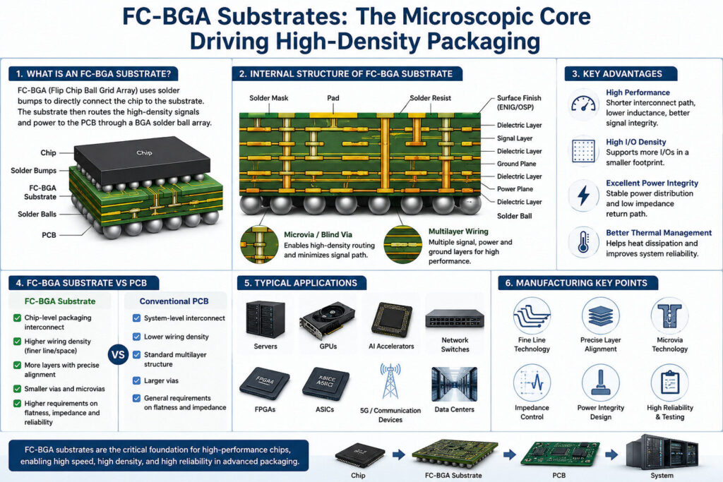
What Is an FC-BGA Substrate?
FC-BGA stands for Flip Chip Ball Grid Array. Unlike traditional wire-bond packaging, flip-chip technology connects the chip directly to the package substrate through solder bumps.
This structure offers several advantages: shorter signal paths, lower parasitic inductance, better electrical performance, and stronger support for high-frequency, high-speed, high-current, and high-I/O chip designs.
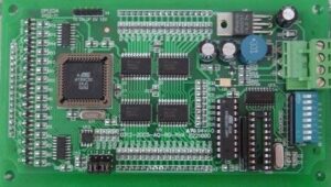
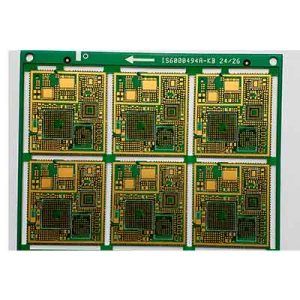
An FC-BGA substrate usually consists of multilayer circuits, dielectric materials, microvias, fine traces, solder mask, pads, and surface finishes. Although it may look like a thin piece of substrate, its internal structure is highly complex. It requires strict control over wiring density, layer-to-layer alignment, impedance, thermal expansion matching, and long-term reliability.
Why High-End Chips Need FC-BGA Substrates
The development of high-performance chips has brought several major changes.
First, the number of chip I/Os is increasing.
CPUs, GPUs, AI chips, switch chips, and high-end processors require a large number of high-speed signal channels, power pins, and ground pins. Without a high-density packaging substrate, it would be difficult to route these connections reliably.
Second, signal speeds are getting faster.
High-speed signals are sensitive to trace length, impedance, crosstalk, and loss. FC-BGA substrates help shorten the signal path and reduce unnecessary interference and signal degradation.
Third, chip power consumption is rising.
High-performance chips draw large currents and generate significant heat. This places higher demands on power integrity and thermal management. An FC-BGA substrate must not only carry signals, but also support power distribution, ground return paths, and heat dissipation.
Fourth, packaging sizes are becoming more compact.
Within limited space, engineers need more connections, higher performance, and better reliability. This is exactly where FC-BGA substrates show their value.
Therefore, an FC-BGA substrate is not just a simple connection carrier. It is a functional platform that plays a key role in high-performance chip packaging.
Key Challenges of FC-BGA Substrates
The difficulty of FC-BGA substrates is not simply making a small board. The real challenge lies in controlling every detail with high precision.
The first challenge is circuit accuracy.
High-density packaging requires finer line width and spacing, smaller vias, and higher layer-to-layer registration accuracy. Even a small deviation may affect signal transmission or cause open circuits, short circuits, or reliability issues.
The second challenge is material matching.
The chip, substrate, solder balls, and PCB all have different coefficients of thermal expansion. During long-term operation, temperature changes can cause stress. If the materials are not properly matched, solder joint fatigue, delamination, or package failure may occur.
The third challenge is impedance and signal integrity control.
In high-speed chip packaging, key signal traces cannot be routed casually. Trace width, dielectric thickness, reference layers, and via structures all affect impedance. For high-speed signals, even a small structural change can create noticeable performance problems.
The fourth challenge is power integrity.
High-performance chips can experience rapid current changes. The substrate must provide stable power paths and low-impedance return paths. Poor power design may lead to power noise, unstable operation, abnormal heating, or system failure.
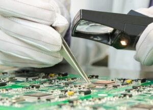
The fifth challenge is manufacturing yield.
FC-BGA substrates have multiple layers, fine circuits, and complex manufacturing processes. Any process variation may affect final yield. This requires advanced equipment, stable process control, strong inspection capability, and extensive engineering experience.
Common Applications of FC-BGA Substrates
FC-BGA substrates are widely used in high-performance, high-density, and high-reliability chip packaging, including:
High-performance CPUs, GPUs, AI accelerator chips, server processors, network switch chips, FPGAs, high-end ASICs, communication base station chips, and data center hardware.
These products share common characteristics: large signal counts, high speeds, high power consumption, and strict reliability requirements.
Traditional packaging methods often struggle to meet these demands. FC-BGA substrates provide shorter interconnection paths, higher I/O density, and better electrical performance, making them an important choice for advanced packaging.
FC-BGA Substrate vs. Conventional PCB
Many people may think of an FC-BGA substrate as a smaller PCB, but the two are very different.
A conventional PCB mainly handles system-level connections between components, such as signal transmission, power distribution, and control circuits.
An FC-BGA substrate handles chip-level packaging connections. It is much closer to the chip and requires finer structures, tighter dimensional control, better flatness, stricter material requirements, and higher reliability.
Conventional PCBs can meet many needs through standard through-holes, multilayer lamination, and impedance control. FC-BGA substrates, however, often require finer traces, smaller microvias, higher layer alignment accuracy, more complex stack-up design, and stricter reliability testing.
In other words, an FC-BGA substrate is not simply a smaller PCB. It is a high-density, high-speed, and high-reliability interconnection platform built at a microscopic scale.
Future Trends: Higher Density, Higher Performance, Stronger Integration
With the rapid growth of AI computing, data centers, high-speed communications, and advanced packaging, the technical requirements for FC-BGA substrates will continue to rise.
Future FC-BGA substrates will develop in several directions.
First, higher circuit density.
As chip I/O counts continue to grow, substrates must support more connections. Line width, spacing, and microvia structures will become even more refined.
Second, better signal integrity.
As high-speed interfaces continue to upgrade, requirements for loss, crosstalk, and impedance continuity will become stricter.
Third, stronger power and thermal performance.
High-power chips require better power distribution and heat management. Substrate design must work closely with the overall packaging and cooling solution.
Fourth, deeper integration with advanced packaging.
Technologies such as chiplets, multi-chip modules, and 2.5D packaging will push FC-BGA substrates toward more complex and higher-end designs.
Conclusion
Although FC-BGA substrates are hidden inside chip packages and are not as visible as the chips themselves, they are a critical part of high-performance electronic systems.
They connect the chip to the motherboard while supporting high-speed signals, power distribution, thermal management, and long-term reliability.
For AI servers, GPUs, communication equipment, high-end industrial systems, and data center hardware, the capability of the FC-BGA substrate directly affects overall system performance and stability.
FC-BGA substrates are not just packaging materials. They are the microscopic core driving high-density packaging and high-performance computing. As chips become more powerful and systems become more complex, the importance of FC-BGA substrates will only continue to grow.