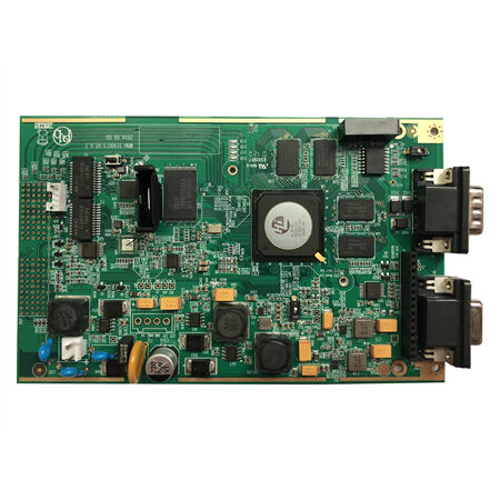
Many customers ask the same question when they first learn about PCB reverse engineering:
“Do you need to destroy the original board?”
This actually involves two different methods: destructive PCB reverse engineering and non-destructive PCB reverse engineering.
Destructive reverse engineering means the board needs to be disassembled layer by layer. Engineers may use methods such as delamination, grinding, layer removal, and photography to restore the traces on each layer of the PCB.
Its advantage is that the cost is relatively lower. It is suitable for simple boards, low-value boards, or projects where the customer has enough original boards. For example, some single-sided boards, double-sided boards, and ordinary control boards can usually be handled this way.
But the disadvantage is also obvious: once the board is opened or ground down, the original board is basically no longer usable. Especially for multilayer boards, high-speed boards, or HDI boards, if there is even a small layer alignment error, the restored circuit may become inaccurate, which can affect later prototyping and testing.
Non-destructive PCB reverse engineering is different. It restores the internal structure and traces of the PCB without damaging the original board, using methods such as X-ray, industrial CT, high-resolution scanning, image modeling, and layer analysis.
Its biggest advantage is that the original board is not destroyed, and the data can be checked repeatedly. It is especially suitable for projects where there is only one original board, the board value is high, or the structure is complicated.
For example, industrial control boards, medical equipment boards, automotive electronics boards, high-speed communication boards, and military-grade boards are often not recommended for destructive reverse engineering. Once these boards are damaged, not only may the design data fail to be restored properly, but the original equipment may also become unusable.
So destructive and non-destructive methods are not simply about which one is better. The right choice depends on the actual project.
If the PCB is simple, there are enough samples, and the goal is only to recover design files, destructive reverse engineering may be more suitable and cost-effective.
But if the PCB is complex, there is only one original board, or the board still needs to be repaired or verified later, non-destructive reverse engineering is usually safer and more reliable.
Professional PCB reverse engineering is not about opening the board immediately or giving a random quote. The first step should be evaluating the board layers, structure, component complexity, whether there is firmware involved, and whether BOM and schematic files are required.
So if you have a PCB that needs design file recovery, you can first send us clear photos of the front and back of the board, the board size, estimated layer count, and your requirements. We can help you determine whether destructive or non-destructive reverse engineering is more suitable, and avoid damaging the original board at the very beginning.