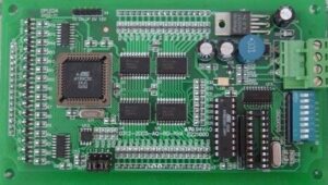
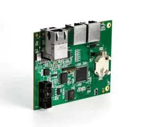
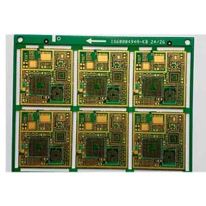
What Is PCB Reverse Engineering?
PCB reverse engineering is the systematic process of extracting design data from a physical printed circuit board. This includes:
- Schematic diagrams — circuit topology and component connections
- Gerber files — manufacturing data for each copper layer
- BOM (Bill of Materials) — complete component list with manufacturers and part numbers
- Stackup data — layer count, dielectric materials, and thickness specifications
- Drill files and netlist data — tooling definitions and signal connectivity
The goal is to produce a complete, producible design package that allows you to manufacture functional replacement boards—or improve upon the original design.
Reverse engineering becomes necessary when the original manufacturer no longer supports a board, when documentation is lost, when you need to reproduce legacy equipment, or when you want to analyze a competitor’s design (with proper authorization).

The Reverse Engineering Process: Where Your Money Goes
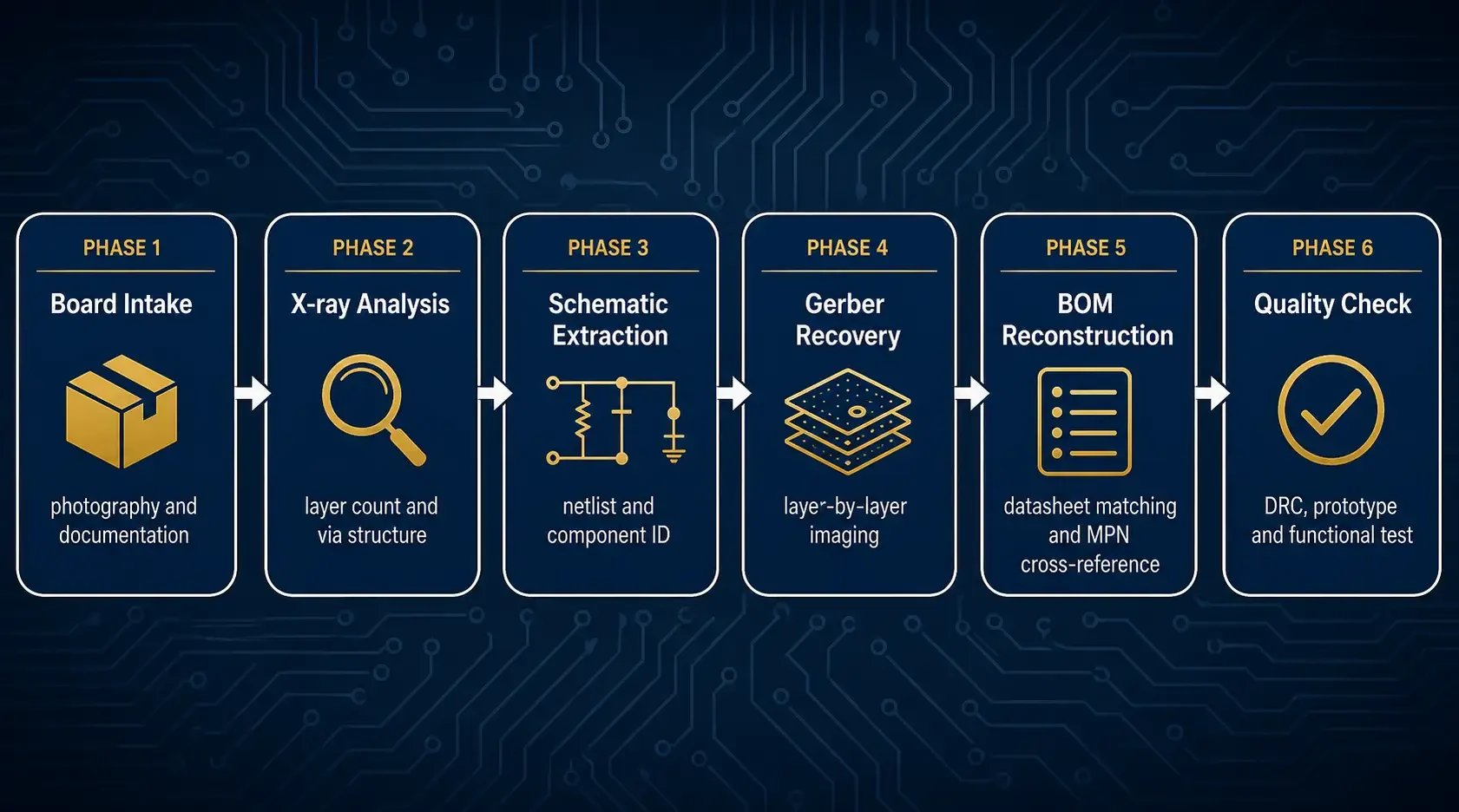
A professional reverse engineering project follows six distinct phases:
Board Intake and Documentation
Thorough incoming inspection with photography, dimension documentation, and serial number recording. Establishes QC baseline.
Duration: 1–2 days | Cost contribution: ~5%
Non-Destructive Analysis (X-ray, Microsection)
X-ray imaging reveals internal layer structure, buried vias, and blind via connections. Cross-sections verify dielectric thickness and copper weight.
Duration: 2–4 days | Cost contribution: ~15–20%
Schematic Extraction
The most labor-intensive phase. Engineers trace every signal path, identify every component, and reconstruct circuit logic. SMT boards require component removal, photography, and database cross-referencing.
Duration: 5–15 days | Cost contribution: ~35–40%
Gerber and Layout Recovery
High-resolution scans (1200+ DPI) regenerate Gerber files including copper traces, solder mask, silkscreen, drill hits, and paste mask data.
Duration: 3–7 days | Cost contribution: ~20–25%
BOM Reconstruction
Identify every component and find exact manufacturer part numbers. For obsolete parts, source alternatives that match electrical and mechanical specifications.
Duration: 2–5 days | Cost contribution: ~10–15%
Quality Verification and Delivery
DRC checks, dimension verification, and prototype functional testing. Delivers complete source files plus professional engineering report.
Duration: 2–3 days | Cost contribution: ~5–10%
2026 PCB Reverse Engineering Cost Breakdown
Tier 1: Simple Boards — $500–$1,200
| Specification | Range |
|---|---|
| Layer count | 1–2 layers |
| Components | < 50 components |
| Package types | Through-hole only, DIP, SIL |
| Board size | < 100mm × 100mm |
| Typical projects | Power supplies, relay boards, simple control cards |
Tier 2: Standard Boards — $1,200–$3,500
| Specification | Range |
|---|---|
| Layer count | 2–4 layers |
| Components | 50–150 components |
| Package types | Through-hole + SOIC, TSSOP, QFP |
| Board size | 100mm × 100mm to 200mm × 150mm |
| Typical projects | Consumer electronics, industrial control boards, automotive sensors |
Tier 3: Complex Boards — $3,500–$8,000
| Specification | Range |
|---|---|
| Layer count | 4–8 layers |
| Components | 150–500 components |
| Package types | BGA (limited pin count), QFN, 0402/0201 passives |
| Typical projects | Communication equipment, motor controllers, medical devices |
Tier 4: HDI / High-Density Boards — $8,000–$15,000
| Specification | Range |
|---|---|
| Layer count | 6–10 layers, HDI construction |
| Components | 300–1,000+ components |
| Package types | Fine-pitch BGA, POP, CSP |
| Typical projects | Smartphones, tablets, high-end networking equipment |
Tier 5: Ultra-Complex / Specialized — $15,000–$30,000+
| Specification | Range |
|---|---|
| Layer count | 10–20+ layers |
| Components | 1,000+ components |
| Package types | Complex BGA stacks, multi-chip modules |
| Typical projects | Military/aerospace, GPU modules, complex industrial systems |
7 Key Factors That Determine Your Reverse Engineering Cost
1. Layer Count and Construction
The single biggest cost driver. Each additional layer adds imaging time, alignment challenges, and complexity to schematic extraction. HDI boards with microvias multiply the cost due to precision requirements.
2. Component Density and Package Types
A board with 200 through-hole resistors is far easier to reverse engineer than one with 200 BGA balls. Fine-pitch BGAs require X-ray analysis to determine pinout, and 01005 passives demand microscope work.
3. Board Size
Larger boards take more imaging passes, generate larger data files, and require more manual tracing work.
4. Deliverables Package
Full Gerber files cost more than schematic-only. The more deliverables required, the more complete the reverse engineering must be.
5. Urgency / Turnaround Time
Standard turnaround is 4–8 weeks. Rush service (2–3 weeks) adds +30–50%. Super-rush (1 week or less) adds +75–100%.
6. Material Analysis Requirements
Specialized materials (high-Tg FR4, polyimide, ceramic, metal core) require cross-section analysis, adding time and cost.
7. Obsolescence and Component Sourcing
Obsolete components require engineering time to find alternatives. Variable cost included in your quote.
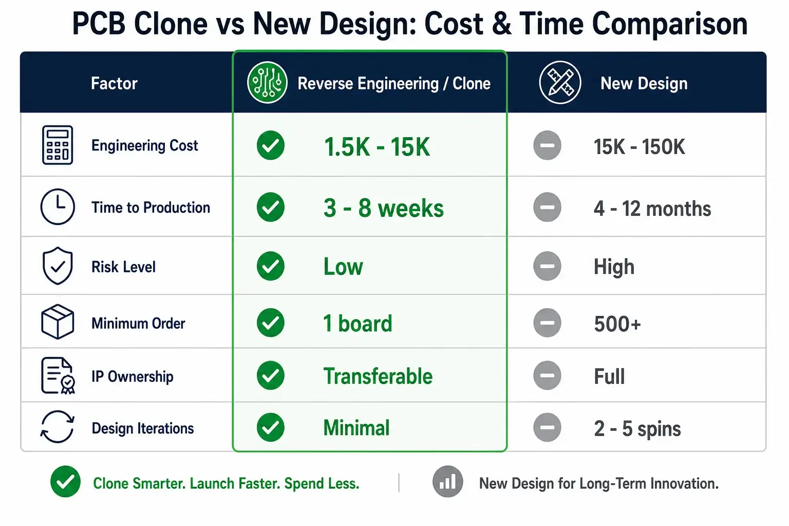
Reverse Engineering vs. New Design: The Real Cost Comparison
| Factor | Reverse Engineering | New Design |
|---|---|---|
| Engineering cost | $1,500–$15,000 | $15,000–$150,000 |
| Time to production | 3–8 weeks | 4–12 months |
| Risk level | Low (proven design) | High (new development) |
| Minimum order quantity | 1 board | 500+ typical |
| IP ownership | Transferable (with agreement) | Full ownership |
| Design iterations | Minimal | Often 2–5 spins |
Case Study: Automotive ECM Reverse Engineering
The challenge: A 2008 heavy-duty truck engine control module failed. OEM replacement: $4,800 and 8-week lead time. Aftermarket: unavailable. Truck down, revenue lost.
The board: 6-layer board, 180mm × 120mm, 280+ components including two BGA chips and several QFP devices, conformal coated.
The process:
- X-ray analysis confirmed 6 layers + 4 buried via structures
- Controlled dehumidity + coating removal
- Component removal and photography (85 components)
- Schematic extraction (est. 340 hours engineering)
- Gerber regeneration for all 6 layers
- BOM creation: 95% exact-match parts, 5% equivalents
- Prototype production and functional testing
- Full replacement board validation
The result: 100% functional replacement board, delivered in 5 weeks, for $6,200. Running flawlessly for 18+ months.
Frequently Asked Questions
How much does PCB reverse engineering cost for a simple board?
For a basic 2–4 layer board with fewer than 100 components and no BGA packages, expect to pay $500–$1,500.
How long does reverse engineering take?
Standard turnaround is 4–8 weeks. Simple boards: 2–3 weeks. Complex HDI boards: 8–12 weeks. Rush service available.
Will I receive Gerber files and a schematic?
Standard deliverables include Gerber files, schematic diagram, BOM, and test reports. Extended packages include ODB++, 3D STEP models, and engineering reports.
What if my components are obsolete?
We source alternatives through major distributors and brokers. Our engineering team identifies drop-in equivalents that meet or exceed original specs. May add 1–2 weeks + small surcharge.
Is my IP protected?
Absolutely. We operate under strict NDA protocols. Your boards and proprietary information are protected throughout. Data transfers to you upon completion.
Can you reverse engineer damaged boards?
Yes. We regularly work with boards that have cracked traces, delaminated layers, burnt components, or missing parts.
Get Your Free Reverse Engineering Quote
Share your board photos and get a detailed, line-item quote within 24 hours.
What we need: Top/bottom board photos, approximate layer count, component estimate, dimensions, required deliverables.
CtrlCpcb – PCB Reverse Engineering & Clone Service Provider | Last updated: 2026-08-13
This article provides general information about PCB reverse engineering costs. Specific costs vary by project complexity, deliverables required, and turnaround time. Obtain detailed quotes for accurate project budgeting.