PCB Copy Services
HUANG TE PCB can clone 1-28 layers PCBs from all kinds of industry, the following is example:
- Various high-end computer motherboards, boards, server motherboards
- Various industrial control motherboards and boards
- High-end network routers, fiber optic network switch motherboards
- Digital TV, DVR, STB, LCD driver motherboard, etc.
- Various wireless base stations and terminal product motherboards
- Various high-precision instruments and equipment motherboards, etc.
- Toys, furniture, machinery, instruments and meters
services
Why Us
HUANG TE PCB’s PCB Cloning Service, is designed to help customers quickly replicate and optimize circuit board designs. With advanced equipment and a skilled engineering team, we accurately restore schematics and BOMs, supporting multilayer boards and high-precision requirements. Whether replacing obsolete products or improving existing designs, we provide efficient and reliable solutions. Choose HUANG TE PCB to make your product development faster and easier!
Save Cost
Market competition is becoming increasingly fierce, and rapid product launch has become the key for companies to gain a foothold in the market. Through PCB copying, companies can make improvements on the basis of original products to avoid designing from scratch, so they can be introduced to the market more quickly and seize opportunities
Save Time
The project cycle is short. In addition to PCB cloning experience, our design team also has a profound manufacturing design background. Manufacturability work allows our PCB copying success rate to reach 100%. At the same time, our PCB and SMT factories are committed to our short cycle. It also provides important protection.
Quality Warranty
PCB copying requires engineers to have an in-depth understanding of circuit principles and wiring. From copying the board to the final product, it needs to go through multiple links such as reverse engineering, simulation analysis, and optimized design. The strength of our technical team is sufficient to ensure that we provide reliable services and products.
Industries We've Copied

Medical

Oil-Gas

Robotics

Sports

Telecom

Aerospace

Agriculture

Automotive

Electronics

Flow
How to Copy a PCB step by step
Record
Get a PCB and first record the model, parameters, and location of all vitality components on paper, especially the direction of the diode, triode, and IC gap.
Layer File
Take the top.bmp/bottom.gmp File to convert to the top.PCB/bottom.PCB, pay attention to convert it to the Drill Guide layer, then just trace the line on the Top layer/Bottom Layer, and place the component package according to the picture. After painting, delete the Drill Guide layer.

Clean
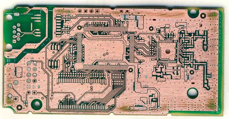
Remove all components and remove the tin from the PAD holes. Use alcohol to clean the PCB, then put it into the scanner, start PHOTOSHOP, and color the silk Scan the printing surface and print it out for later use.

Polish & Scan
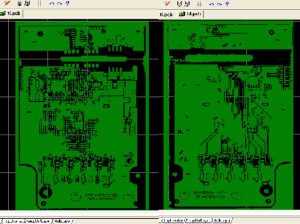
Lightly polish the TOPLAYER and BOTTOMLAYER layers with water gauze paper until the copper film is shiny. Put it in the scanner, start PHOTOSHOP, and scan the two layers in color. Note that the PCB must be placed horizontally and vertically in the scanner, otherwise the scanned image will not be usable.

Copy
Adjust the contrast and lightness of the canvas so that the part with copper film and the part without copper film are in strong contrast. Then convert the image to black and white and check whether the lines are clear. If not, repeat this step. If it is clear, save the image as black and white BMP format files TOP.BMP and BOT.BMP.

Convert
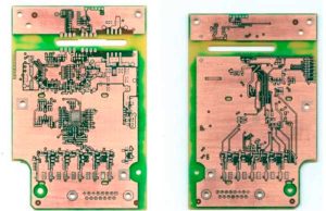
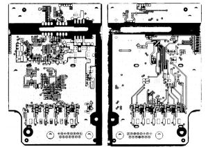
Convert the two BMP format files to PROTEL format files respectively, and transfer the two layers in PROTEL. The positions of PAD and VIA on the two layers are basically coincident, indicating that the first few steps are done well. If there is a deviation, repeat the third step.

PCB File
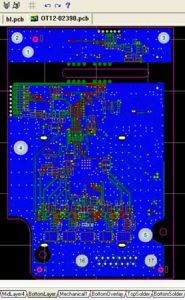
Set TOP in PROTEL. PCB and BOT. PCB is transferred in and merged into one picture and it is OK.

Inspection
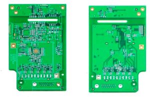
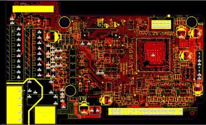
Inspection. After drawing all the layers, you still need to check carefully. Export the drawn PCB file as a GERBER file, open it through CAM2000DE, then export the picture and compare it with your PCB source file to see if there are any omissions or errors.