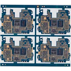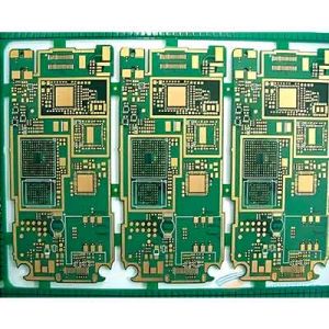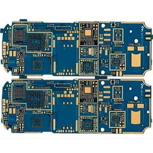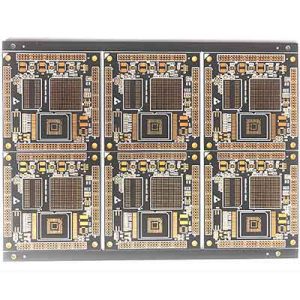
High-Performance HDI PCB Manufacturing
Advanced solutions for compact, high-speed, and reliable electronics.
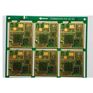
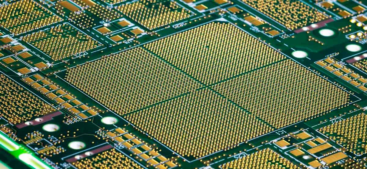
At HUANG TE PCB, we specialize in manufacturing High Density Interconnect (HDI) PCBs with precise multilayer structures, microvia technology, and advanced materials to meet the demands of modern electronic products.
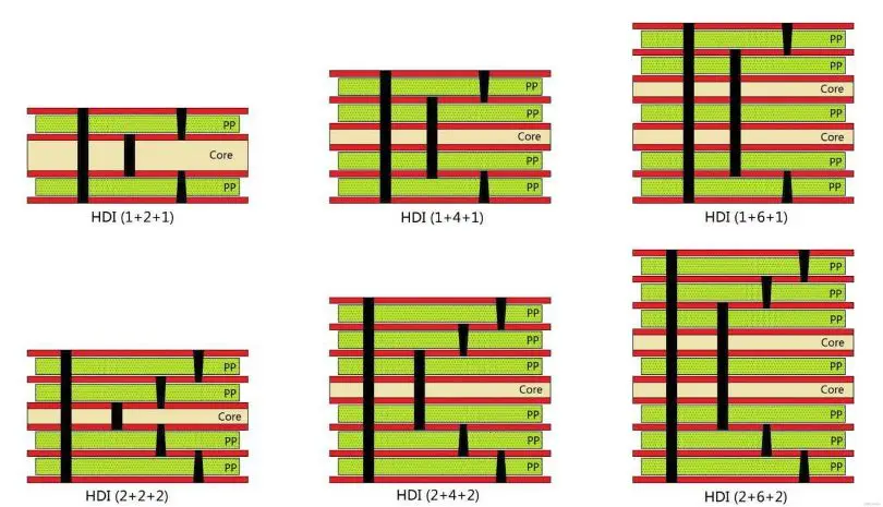
Common Buildup Structure
The difference between HDI PCB and ordinary PCB, you can see from the Buildup Structure.
The Stackup show 1+ N +1 and 2+N+2 HDI PCB Structure
HDI PCB vs. Traditional PCB
| Feature / Parameter | HDI PCB (High Density Interconnect) | Traditional PCB |
|---|---|---|
| Line/Space | As low as 50 μm (0.05 mm) | Typically ≥ 100 μm |
| Via Technology | Microvias, blind vias, buried vias, via-in-pad | Through-hole vias only |
| Layer Count | Up to 20+ layers with compact design | Usually up to 8–12 layers |
| Density | High component density, compact design | Lower density, larger board size |
| Signal Integrity | Better performance for high-speed & RF circuits | More signal loss and crosstalk |
| Size & Weight | Smaller, lighter, space-saving | Larger and heavier |
| Design Flexibility | Allows advanced stack-ups (1+N+1, 2+N+2, any-layer) | Limited stack-up options |
| Applications | Smartphones, tablets, medical devices, automotive, aerospace | Consumer electronics, industrial equipment, home appliances |
| Manufacturing Cost | Higher (advanced process required) | Lower |
| Reliability | High reliability, especially for portable and high-frequency devices | Standard reliability |
Over 30 years of PCB manufacturing experience
Advanced HDI production lines with strict quality control
In-house testing & reliability verification (X-ray, AOI, impedance test, etc.)
Fast prototyping & mass production services
Strong engineering team supporting DFM (Design for Manufacturability)
Laser-drilled microvias (blind & buried)
1+N+1, 2+N+2, and any-layer HDI stack-up options
Minimum line/space: 50 μm
Via-in-pad & filled via technology
High layer count (up to 20+ layers)
Advanced surface finishes (ENIG, Immersion Silver, Hard Gold, etc.)
Reliable material options: Rogers, Panasonic, Isola, etc.
HDI PCBs bring multiple benefits compared to standard PCBs, including:
Higher component density for compact design
Improved signal integrity & reduced crosstalk
Enhanced electrical performance for high-speed circuits
Lightweight and space-saving for portable devices
Greater design flexibility
Our HDI PCBs are widely used in:
Smartphones & tablets
Automotive electronics & ADAS systems
Medical devices & wearable technology
Network & communication equipment
Consumer electronics
Aerospace & defense systems
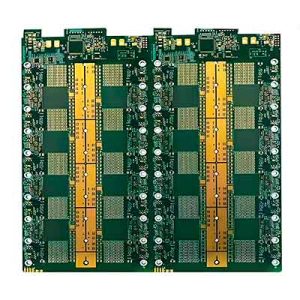
Multi-Layer PCB Manufacturing Capability