What Is Rigid Flex PCB Stackup?
Rigid flex PCB stackup refers to the layered construction that integrates rigid FR4 sections with flexible polyimide circuits in a single laminated structure. Unlike traditional rigid PCB where all layers are the same material system, rigid flex must accommodate two fundamentally different material types with different mechanical properties and thermal expansion characteristics. The Global Electronics Association (formerly IPC) defines rigid flex requirements in IPC-6013, the qualification specification that establishes stackup construction standards and performance requirements.
The stackup design is the foundation of any rigid flex PCB. It determines not only the electrical performance—impedance control, signal integrity, and power distribution—but also the mechanical performance including flexibility, bend radius capability, and long-term reliability. A well-designed stackup balances electrical requirements with manufacturing feasibility and cost constraints. The interaction between rigid and flexible sections creates unique design challenges that do not exist in standard rigid PCB design.
Stackup design directly impacts manufacturing yield and cost. Configurations that are difficult to manufacture result in lower yields and higher per-unit costs. Working with your manufacturer during stackup selection helps identify designs that meet electrical requirements while remaining manufacturable at target volumes. The optimal stackup for your application depends on layer count requirements, signal integrity needs, flexibility requirements, thermal environment, and budget constraints.
Stackup Layer Configurations
Rigid flex configurations range from simple 2-layer designs to complex 8-layer or higher constructions. Each configuration serves different application requirements, and selecting the appropriate layer count is the first decision in stackup design. The number of rigid layers, flex layers, and their arrangement defines the board’s capabilities and limitations. Higher layer counts provide more routing flexibility and better signal integrity but increase cost and manufacturing complexity.
| Configuration | Rigid Layers | Flex Layers | Total Layers | Typical Application |
|---|---|---|---|---|
| 2-Layer Rigid Flex | 1 | 1 | 2 | Simple point-to-point interconnects |
| 4-Layer Rigid Flex | 2 | 2 | 4 | Standard applications, moderate routing |
| 6-Layer Rigid Flex | 4 | 2 | 6 | Complex routing, power distribution |
| 8-Layer Rigid Flex | 6 | 2 | 8 | High-density, multi-component |
Rigid flex PCB cost increases significantly with layer count, making it important to select the minimum configuration that meets your requirements. A 2-layer rigid flex provides basic connectivity between rigid sections with one routing layer in each. While simple, this configuration is often sufficient for applications like LED arrays or simple sensor connections where limited routing is required. The manufacturing process for 2-layer rigid flex is the most straightforward, resulting in the lowest cost premium over equivalent rigid PCB.
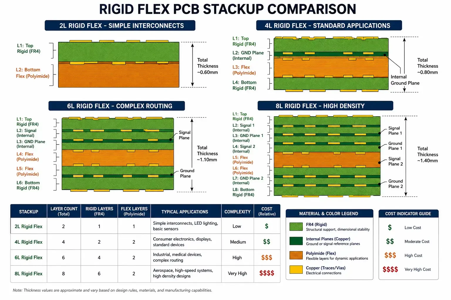
4-layer rigid flex is the most common configuration for general applications. With two rigid layers and two flex layers, this configuration provides one dedicated ground plane, one dedicated power plane (in the rigid section), and two routing layers that can extend into flex areas. The ground plane extending into flex areas provides shielding and consistent impedance for signals crossing between rigid and flex sections. This configuration balances cost, manufacturing complexity, and electrical performance for most applications including consumer electronics and industrial controls.
6-layer and 8-layer configurations serve high-density applications with complex routing requirements. These multilayer rigid flex designs enable multiple ground planes, distributed power planes, and complex signal routing that would be impossible in simpler configurations. However, the manufacturing complexity increases substantially with each additional layer. Multiple lamination cycles may be required, each introducing yield risk and cost. These configurations are typically reserved for aerospace, medical, and high-end computing applications where the performance benefits justify the additional cost and manufacturing challenge.
Materials in Rigid Flex Stackup
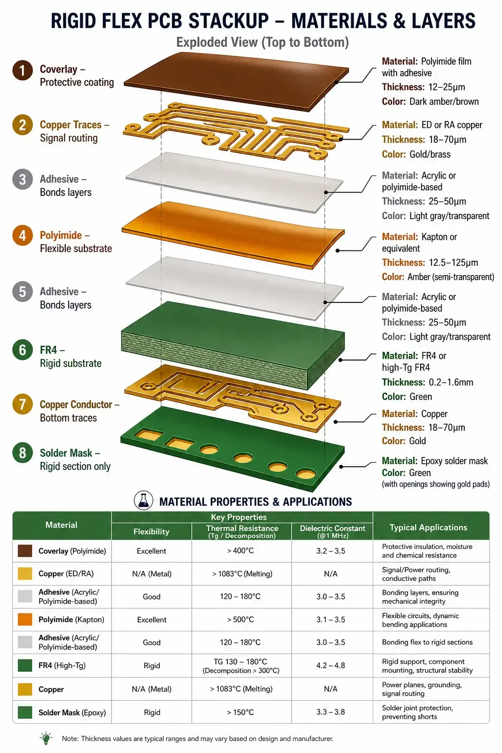
Material selection defines the performance boundaries of any rigid flex stackup. The combination of rigid and flexible materials in a single structure creates unique challenges that require careful material matching. Each material layer serves a specific purpose, and the interaction between layers determines overall board reliability. Understanding material properties helps engineers make informed stackup decisions that balance performance, cost, and manufacturability.
Rigid sections typically use FR4 or high-Tg FR4 as the base substrate. Standard FR4 provides adequate performance for most applications at the lowest cost. High-Tg FR4, with glass transition temperatures of 150°C or higher, is used when the assembly will be exposed to elevated temperatures during soldering or operation. The rigid material provides mechanical strength for component mounting and provides the stable platform required for surface mount assembly. Rigid section thickness typically ranges from 0.2mm for thin applications to 1.6mm for high-component-weight designs.
Flexible sections use polyimide film as the base material, with DuPont Kapton being the industry standard since the 1970s. Polyimide provides the exceptional flexibility and thermal resistance required for flex circuits. Available thicknesses range from 12.5μm for maximum flexibility to 125μm for applications requiring more robust flex areas. Thinner films achieve tighter bend radii but have lower dielectric strength. The polyimide film is clad with electrodeposited (ED) or rolled (RA) copper conductor, with RA copper preferred for dynamic flex applications due to its superior flex fatigue resistance.
Adhesive systems bond rigid and flex layers together, representing one of the most critical material choices in rigid flex design. Acrylic adhesives provide cost-effective bonding with good flexibility, making them suitable for static flex applications. Polyimide-based adhesives offer superior thermal resistance and are preferred for applications involving multiple high-temperature assembly cycles or sustained high-temperature operation. Adhesive thickness, typically 25-50μm, affects overall stackup thickness and must be accounted for in bend radius calculations. The adhesive must remain flexible throughout the product lifecycle without becoming brittle or delaminating.
Coverlay protects exposed conductors in flex areas, serving the same function as solder mask in rigid PCB. Coverlay is typically 12-25μm polyimide film with pressure-sensitive adhesive, applied over circuit traces in flex zones. Coverlay provides mechanical protection, electrical insulation, and environmental resistance. The coverlay should be omitted or carefully designed in tight bend zones where its additional thickness would restrict flexibility. Coverlay versus solder mask considerations are important for flex area design.
Rigid-to-Flex Transition Design
The rigid-to-flex transition zone is the most critical and sensitive area in any rigid flex PCB design. This is where the mechanical properties change abruptly from the stiff rigid section to the flexible polyimide section. According to IPC-2223 design standards, the transition zone requires careful attention to prevent stress concentration that causes delamination, cracking, or conductor fatigue. Failure in the transition zone is the most common failure mode in rigid flex circuits.
Stress concentration at the transition line is the primary concern. When the board bends, stress concentrates at the boundary where the rigid material meets the flexible material. Without proper design, this stress concentration leads to crack initiation in conductors and adhesive failure at the interface. Design strategies to reduce stress concentration include creating a gradual transition rather than an abrupt change, using strain-relief features such as additional adhesive patches or encapsulation, and ensuring smooth radius transitions at all edges.
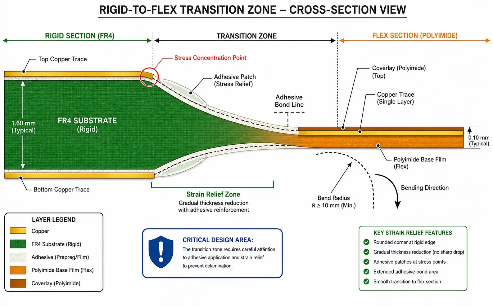
Adhesive application in the transition zone requires special attention. The adhesive must bond rigid and flex layers without creating a stress concentration point. Too much adhesive in the transition creates a thick, stiff area that defeats the purpose of the flex section. Too little adhesive creates a weak bond prone to delamination. Manufacturers typically specify the minimum adhesive coverage and location requirements for reliable transition zone construction. The adhesive should extend well into the rigid section to ensure robust bonding while being gradually reduced before reaching the active flex area.
Stiffener attachment at transition zones provides additional reinforcement. Stiffeners made from FR4 or polyimide are bonded to the flex circuit at termination points, extending into the rigid section to create a gradual stiffness gradient. The stiffener thickness and length determine the stress distribution in the transition. Typical stiffener extension into the flex area is 3-5mm minimum, with thicker stiffeners required for higher-stress applications. The stiffener edge should use a radiused transition rather than a sharp corner to further reduce stress concentration.
Component placement near transition zones requires careful consideration. Components mounted too close to the transition experience stress from board bending that can lead to solder joint failures. Industry practice recommends maintaining minimum clearances between component pads and the transition line. For high-vibration applications or products with ongoing flexing, these clearances should be increased to account for cumulative stress over the product lifecycle.
Signal Integrity in Stackup Design
Signal integrity in rigid flex requires attention to layer assignment, trace routing, and impedance control across both rigid and flex sections. The transition between rigid and flex areas creates discontinuities that can degrade signal quality if not properly managed. For high-speed applications, signal integrity considerations often drive stackup selection and layer assignment decisions. Engineers must verify that controlled impedance requirements are met in both the rigid and flex portions of the board.
Ground plane extension into flex areas provides consistent reference for signal traces crossing between rigid and flex sections. The ground plane maintains trace geometry during bending, ensuring consistent impedance. Without ground plane reference in the flex area, trace impedance varies with bending, potentially exceeding tolerance limits. Ground plane coverage in flex areas should match or exceed the coverage in adjacent rigid sections to maintain consistent return current paths.
Trace routing in flex zones requires attention to bend axis orientation. Traces running perpendicular to the bend axis experience lower strain than traces running parallel to the bend axis. For dynamic flex applications requiring repeated bending, traces should be routed perpendicular to the bend axis where possible, and widths should be minimized in high-strain areas. Flex PCB bend radius requirements directly affect trace routing in flex zones.
Controlled impedance in rigid flex presents unique challenges. The impedance calculation must account for the different dielectric properties of rigid and flex materials. Flex area impedance may differ from rigid area impedance even for the same trace geometry due to differences in material properties. Verification testing of impedance values in flex areas is recommended for high-speed designs. Time domain reflectometry (TDR) testing can verify impedance continuity across rigid-to-flex transitions.
Common Applications by Stackup Configuration
Different applications require different stackup configurations based on complexity, reliability requirements, and environmental exposure. Matching the stackup to the application ensures adequate performance while avoiding over-specification that increases cost unnecessarily. Understanding typical stackup requirements for common applications provides a starting point for stackup selection.
Consumer electronics including smartphones and wearables typically use 4-layer rigid flex configurations. The rigid sections mount processors, memory, and connectors while the flex section connects display modules, batteries, and cameras. Space constraints drive aggressive component density, requiring the routing flexibility of 4-layer designs. Consumer products prioritize cost optimization, making 4-layer configurations the sweet spot for performance versus cost. Dynamic flex applications like foldable phones may require higher layer counts for complex routing.
Automotive applications favor 4-layer to 6-layer rigid flex with high-reliability materials. Automotive requirements include extended temperature range operation, vibration resistance, and long lifecycle expectations. High-Tg FR4 materials provide thermal stability during engine compartment mounting, and robust transition zone design ensures reliability despite continuous vehicle vibration. Automotive electronics increasingly use rigid flex to reduce weight and eliminate cable connectors that could loosen under vibration.
Medical devices range from 2-layer to 6-layer configurations depending on complexity and sterilization requirements. Implantable devices often use simple 2-layer rigid flex to minimize size, while diagnostic equipment may require 4-6 layers for complex signal processing. Medical applications prioritize reliability and miniaturization, making rigid flex ideal for pacemakers, hearing aids, and imaging equipment. Material selection for medical applications must consider biocompatibility and sterilization compatibility.
Aerospace and defense applications typically use 6-layer to 8-layer rigid flex with specialized high-reliability materials. These demanding applications require multilayer constructions for complex routing, redundant power distribution, and extensive ground plane coverage. Spacecraft and satellite applications additionally require radiation-tolerant materials and specific outgassing characteristics. The extreme reliability requirements justify the higher cost and manufacturing complexity of multilayer rigid flex.
Common Mistakes to Avoid
Selecting inappropriate layer count is the most common stackup error. Over-specifying layer count wastes cost; under-specifying creates routing congestion that compromises signal integrity or forces layout compromises. Start with the minimum layer count that meets your routing and impedance requirements, and increase only when justified by specific electrical needs. The cost difference between 4-layer and 6-layer rigid flex is substantial and should not be incurred without clear technical justification.
Ignoring material compatibility leads to reliability failures in the field. Materials with mismatched thermal expansion coefficients create stress during temperature cycling that causes delamination or cracking. Verify that all materials in your stackup are compatible with your thermal environment, assembly processes, and operating temperature range. This includes the rigid and flex materials, adhesives, and any surface finishes applied to the board.
Underestimating transition zone requirements causes premature failure at the rigid-to-flex interface. The transition zone is not just a boundary—it requires deliberate design for strain relief, adhesive application, and stiffener attachment. Designs that treat the transition as a simple boundary between two materials will fail under thermal cycling or mechanical stress. Allocate appropriate design resources to transition zone optimization.
Frequently Asked Questions
What is rigid flex PCB stackup?
Rigid flex PCB stackup refers to the layered construction combining rigid FR4 sections with flexible polyimide circuits in a single integrated board. Per IPC-6013, the stackup defines the arrangement, thickness, and materials of each layer including rigid substrates, flex cores, adhesive layers, and coverlay. The stackup design determines electrical performance, mechanical flexibility, and manufacturing requirements.
How many layers does rigid flex PCB need?
Rigid flex layer count depends on application requirements. Simple interconnects may use 2-layer rigid flex with one flex layer. Standard applications typically require 4-layer rigid flex with two flex layers for routing flexibility. Complex high-density designs may need 6-8 layers. Higher layer counts increase cost and manufacturing complexity but provide more routing options and better signal integrity.
What materials are used in rigid flex PCB stackup?
Rigid flex stackup uses multiple material types. Rigid sections use FR4 or high-Tg FR4 substrates. Flex sections use polyimide film (such as DuPont Kapton) as the base material. Adhesive layers bond rigid and flex materials together, typically acrylic or polyimide-based. Coverlay protects exposed conductors in flex areas. Material selection depends on thermal requirements, flexibility needs, and cost constraints.
What is the rigid-to-flex transition zone?
The rigid-to-flex transition zone is the critical interface where rigid FR4 meets flexible polyimide. Per IPC-2223, this transition requires careful design to prevent stress concentration that causes delamination or cracking. Design considerations include gradual thickness changes, proper adhesive application, and adequate strain relief. The transition zone is typically the most sensitive area for rigid flex reliability.
How to design rigid flex stackup for signal integrity?
Signal integrity in rigid flex requires proper layer assignment. Ground planes should extend into flex areas to provide consistent impedance and shielding. Signal traces in flex zones should be perpendicular to bend axes where possible. Reference planes maintain trace geometry during bending. For high-speed signals, controlled impedance requirements must be verified in both rigid and flex sections.
What are common rigid flex stackup configurations?
Common rigid flex configurations include: 2-layer (1 rigid + 1 flex) for simple connections; 4-layer (2 rigid + 2 flex) for standard applications; 6-layer (4 rigid + 2 flex) for complex routing; and 8-layer (6 rigid + 2 flex) for high-density designs. Each configuration has specific material and manufacturing requirements defined in IPC-6013.
References
- Global Electronics Association. IPC-6013E Qualification and Performance Specification for Flexible Rigid Printed Boards. https://electronics.org/
- Global Electronics Association. IPC-2223E Sectional Design Standard for Flexible/Rigid-Flexible Printed Boards. https://electronics.org/
- DuPont Electronics & Industrial. Kapton Polyimide Film Product Information. https://www.dupont.com/
Further Reading
- Flex PCB Bend Radius: Complete Guide to Minimum Bending Radius | Learn about minimum bend radius requirements for flex circuits
- Polyimide vs LCP vs PET Flex PCB: Material Comparison Guide | Compare base film materials for flex circuits
- Rigid Flex PCB Cost: Price Factors and Cost Optimization Guide | Understand cost implications of different stackups
Shanghai Huangte Technology Co., Ltd. | Last updated: 2026-08-04
This article provides general guidance on rigid flex PCB stackup design based on industry standards and manufacturer specifications. For specific applications, consult with your PCB manufacturer to validate stackup selection and obtain manufacturing recommendations for your particular construction requirements.