Power Supply PCB Manufacturer
The printed circuit board power supply is the circuit that is connected to a power source. Power Supply PCB controls the amount of voltage and current delivered to printed circuit board. The power delivered can either be alternating current (AC) or direct current (DC). The power supply PCB converts the input voltage from the power source into the output voltage required by the electronic equipment. This circuit regulates the current flow to ensure that the electronic device receives the appropriate amount of power. It is an important component of any electronic equipment that requires a power source to function. A power supply PCB is designed to distribute and regulate power to electronic devices.
Types of Power Supply PCBs
Power supply printed circuit boards need power to function. Usually this is achieved with the onboard power supply feature. Power supply PCBs have two major types according to their operation.
Linear Power Supplies PCB
This type of power supply PCB converts alternating current (AC) into direct current (DC) using a transformer. Furthermore, linear power supply PCBs are more efficient and reliable. These power supply PCBs are large and bulky. So, they are preferred for electronic applications that are not weight- and size-sensitive. Linear power supply PCB is widely used in industrial systems.
Such power supplies are low cost and simple to design onto a printed circuit board. They are used in systems where lower power is required.
Switch Mode Power Supply (SMPS) PCB
The second type of power supply PCB is switch mode power supplies that convert AC to DC by using transistors. Unlike linear power supply PCBs, switched mode power supply PCBs are smaller and lighter. Therefore, they are more preferred to be used in applications such as computers and cell phones where weight and size matter. They are more efficient than linear power supply PCBs. But their designing is more complex and their switching noise can create electromagnetic interference (EMI) issues, if proper attention has not cared.
SMPSs are categorized into isolated and non-isolated power supply PCB.
Key Components & Design Consideration of a Power Supply PCB
- Layer Stackup
- Trace Routing
- Grounding Components and Power Plane
- Component Placement
- Trace Spacing and Width
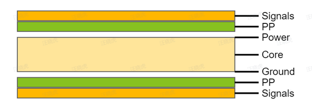
When designing a power supply PCB, the layer stackup component is crucial to consider. In a multi-layer circuit board configuration, there should be a power plane or ground between the routing and outer layer with power supply components and the inner layer with sensitive signals. The power plane will work as a shield to safeguard the sensitive signal traces from noisy power components.

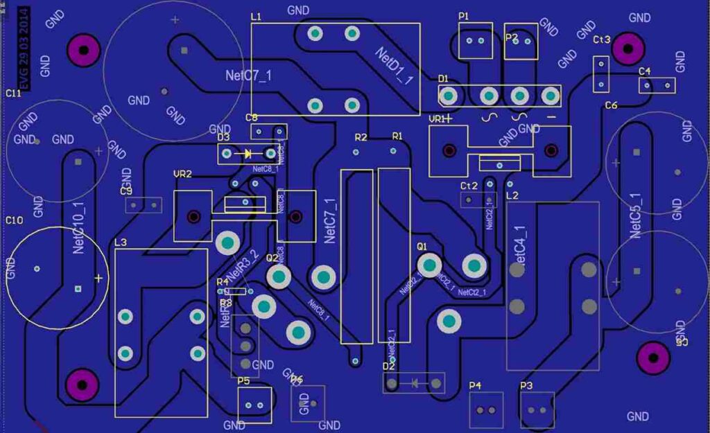
Trace routing is a critical component of power supply PCB design, as it directly affects the performance, efficiency, and safety of printed circuit board power supply. Power paths, current paths, signal traces, and via placement are important factors in trace routing of power supply PCB design.
Designing a power supply PCB needs to create a separate ground for the power supply PCB components. This will not only provide optimal grounding for the power supply, but it will also separate the noise of the current paths. Commonly, two ground planes are connected at a single point, which is usually the ground via in the thermal pad. Power planes and grounding are important components of any power supply PCB. Ground planes offer a low-impedance return path to the flow of current, while power planes provide a low-impedance power source.

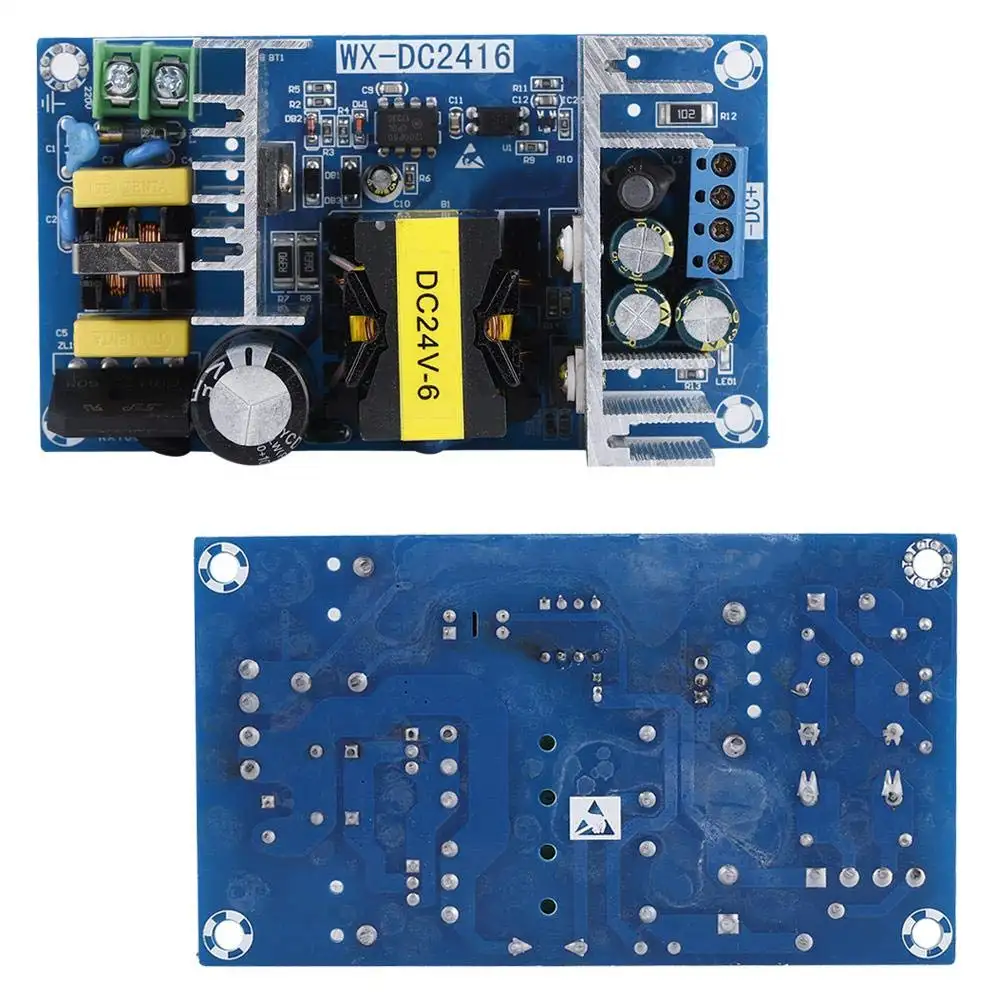
Component placement on a power supply PCB is crucial for maintaining proper operation and reducing signal noise. Power supply and other components in printed circuit board power supply design should be placed close together to minimize parasitic capacitance and reduce trace length and inductance.

Trace spacing and width on a power supply PCB are also crucial factors and design considerations. Trace widths must be enough to handle the specific current without causing excessive heat or voltage drops. Trace spacing should also be sufficient to avoid arcing or short circuits, specifically in high-voltage applications of printed circuit boards.
Testing & Troubleshooting of Power Supply PCBs
- Power On Testing
- Functional Testing
- Signal Integrity Testing of Power Supply PCB
- Debugging Techniques
- Commonly use a variable power supply to gradually increase voltage drop.
- Check for excessive current flow, which can cause a short circuit in printed circuit board.
- Use an infrared thermometer to identify overheating components in the power supply PCB.
This is a very basic test that is performed on the power supply PCB design. It includes the following steps.
- Ensure that printed circuit board power supply produces the accurate voltage.
- Requires a load resistor and multimeter
- Connect the multimeter to the output side.
- Check if the output voltage is within an acceptable range, then the power supply PCB is functioning correctly.
The purpose of this test is to check whether the power supply produces stable and clean power.
- It involves measuring noise levels and ripples on output terminals.
- Requires a load resistor and an oscilloscope.
- Connect the oscilloscope at the output terminals and adjust the load resistor to match the expected load.
- If the noise and ripple are within acceptable limits, the power supply is stable.
Debugging a power supply PCB is a complex task that involves identifying and fixing errors and faults to restore proper functionality of printed circuit board power supply. This includes the following steps.
- Using a schematic diagram helps to find the power flow through the circuit.
- Debugging helps in identifying faulty components such as ICs, resistors, and capacitors.
- Verifies the voltage levels at different test points.
- Makes a power path from the input to the output terminal.
- Debugging techniques make it easier to find open circuits, short circuits, and incorrect connections.
- Important for efficient repair and systematic troubleshooting