


PCB Layout Design Services
services
Our PCB Layout Services Content
We offer a wide range of services, including:
- Schematic Capture: We convert your circuit ideas into a detailed schematic diagram.
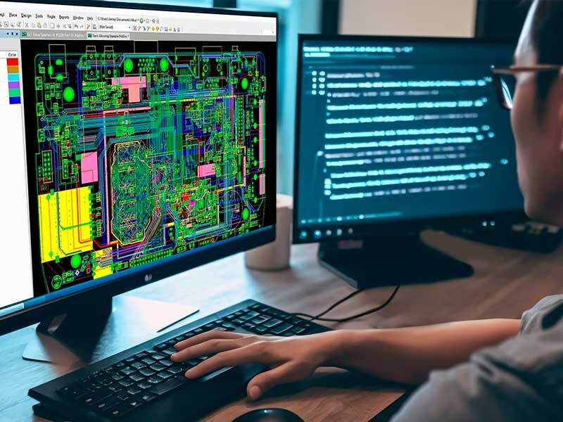
- PCB Layout Design: We design the physical layout of the PCB, optimizing for performance, reliability, and manufacturability.
- Design for Manufacturing (DFM): We ensure that your design is ready for efficient and cost-effective production.
- Fabrication Files: We generate manufacturing files for you, like Gerber files.
- Prototype Testing: We can assist with prototype testing to verify the functionality and performance of the design.
- Production Run: We also provide PCB Manufacturing and Assembly Services for your production run.
PCB Layout Software we use
Altium Designer
Allegro
OrCad
PCB Layout Services Process
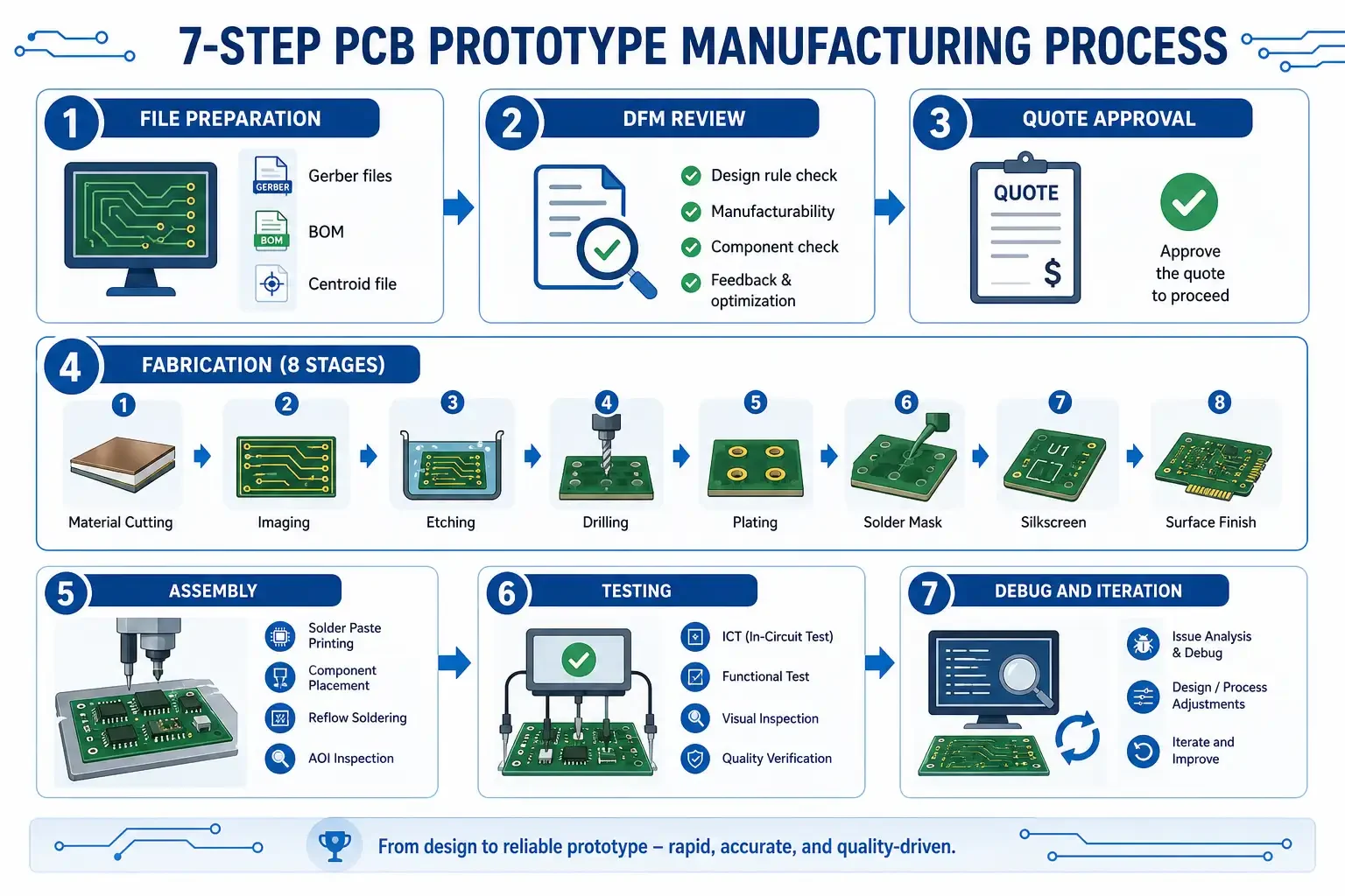
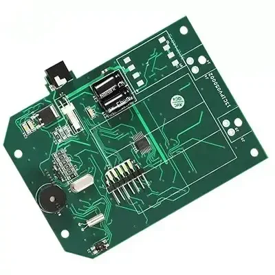
The creation of a PCB layout is a detailed procedure that involves converting a schematic into a physical blueprint, deciding the location of each component on the board, and establishing the interconnections among them. Here are the primary stages involved in formulating a PCB layout:
Schematic Design: The journey begins with the creation of a detailed schematic diagram of your circuit.
Component Placement: The subsequent stage involves determining the location of each component on the board.
Routing: This stage involves the creation of paths (traces) that electrically interconnect the components.
Design Rule Check (DRC): This is a process automated by software that checks if the layout adheres to the rules set by the PCB fabrication house.
Gerber Generation: The final stage involves the generation of Gerber files, which are the standard file format for manufacturing PCBs.
In addition to these stages, there are several factors to consider during the PCB layout process:
Component Placement Optimization: Components should be strategically placed to minimize trace lengths and prevent crossing signal paths.
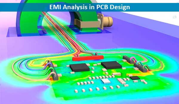
Signal Traces and Routing: Special care should be taken to avoid signal integrity issues such as crosstalk and electromagnetic interference.
Thermal Considerations: The layout should consider heat dissipation, especially for high-power components.
Ground Plane Design: A well-designed ground plane can help reduce noise and improve signal integrity.
Design Rule Checks (DRCs): Regular DRCs should be conducted throughout the design process to identify and correct errors early.
Manufacturer Collaboration: Close collaboration with the PCB manufacturer can help ensure the design is optimized for manufacturability.
Remember, the design of a PCB layout requires careful planning, meticulous attention to detail, and compliance with industry standards and guidelines. I hope this provides a comprehensive overview of the PCB layout process. If you have any more questions, don’t hesitate to ask!
PCB Layout Services Process
Expertise
Our team has extensive experience in PCB design across various industries and applications.
Quality
We adhere to strict quality standards to ensure the reliability and longevity of your products
Efficiency
We use advanced design tools and techniques to optimize the design process and reduce time-to-market.
Support
We provide ongoing support throughout the design process, from initial concept to final production.
PCB Layout Services Process

PCB Redesign vs Clone — Complete Decision Guide 2026
PCB clone vs redesign is the core decision when a board reaches end-of-life. Clone recovers

orm Fit Function Replacement PCB — Pin-Compatible Component Sourcing Service
Form-fit-function (FFF) replacement is the targeted, lowest-cost method for replacing obsolete PCB components with pin-compatible

Obsolete PCB Replacement — End-of-Life Board Replacement Service 2026
Obsolete PCB replacement is the service of reproducing or substituting a printed circuit board that

Multilayer PCB Clone Service — 2L to 16L+ Cloning from Physical Boards 2026
Multilayer PCB clone service recovers a complete design package — Gerber, schematic, BOM, and stackup

PCB BOM Reconstruction — Complete Bill of Materials Recovery Guide 2026
PCB BOM reconstruction is the process of identifying every component on a physical PCB and

How to Recover Schematic from PCB — Professional Extraction Methods 2026
Recovering a schematic from a physical PCB is a multi-stage reverse engineering process that combines

Recover Gerber Files from PCB
Recovering Gerber files from a physical PCB involves a multi-stage process combining optical scanning for

X-ray PCB Reverse Engineering
X-ray PCB reverse engineering enables non-destructive imaging of multilayer boards, revealing internal copper routing, via

PCB Reverse Engineering Deliverables
PCB reverse engineering deliverables are the complete set of design files produced from analyzing your