


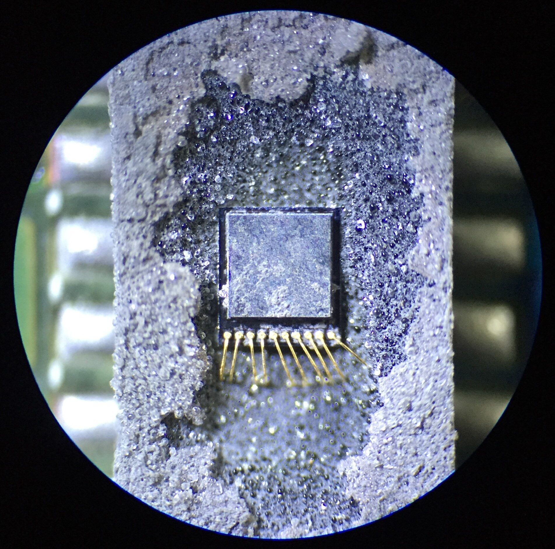
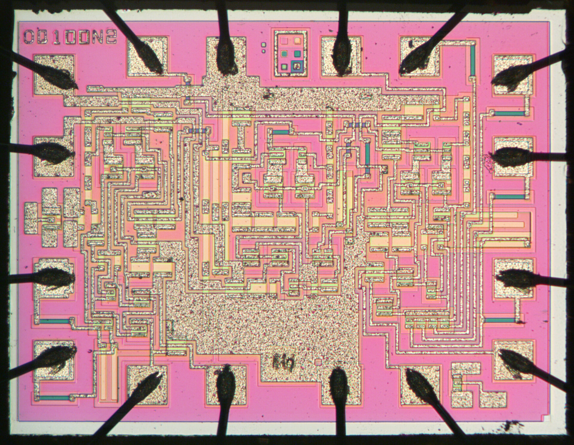
Advanced Chip Decapsulation and IC Failure Analysis
Advanced Chip Decapsulation and IC Failure Analysis High-Precision Chip Decap Technology Integrated circuits are the
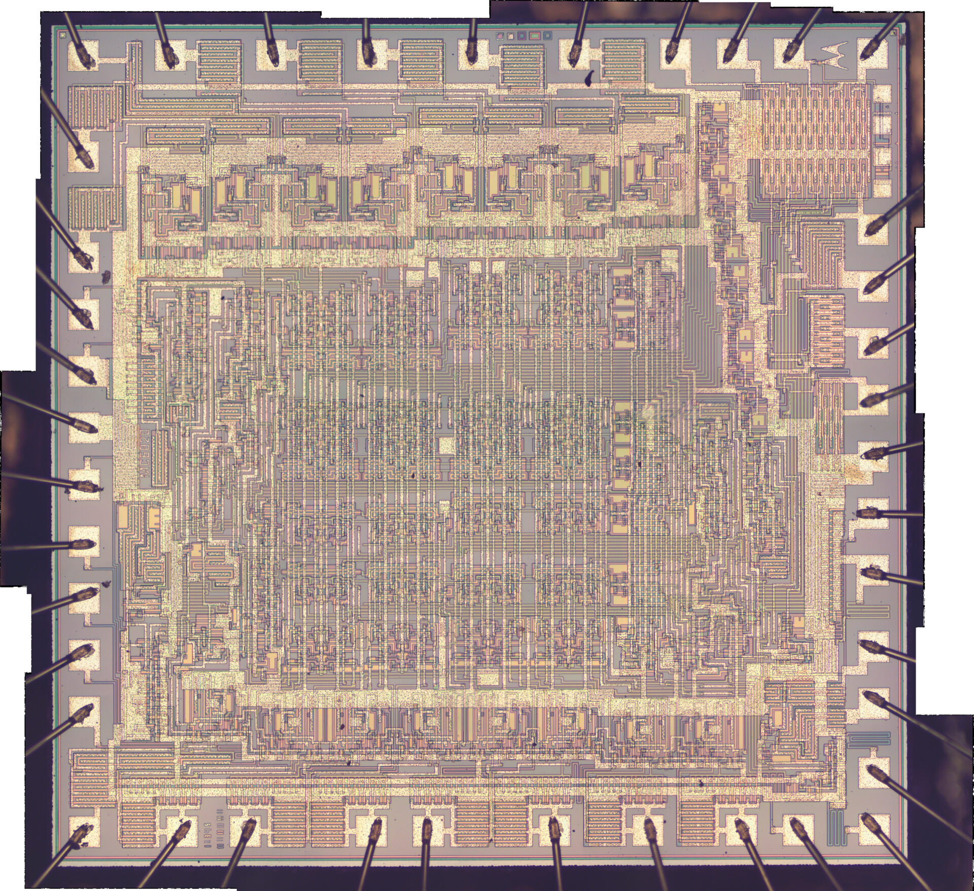
Advanced Chip Reverse| Engineering Case Study
Advanced Chip Reverse Engineering Case Study Modern electronic devices rely heavily on semiconductor chips. When
.jpg)
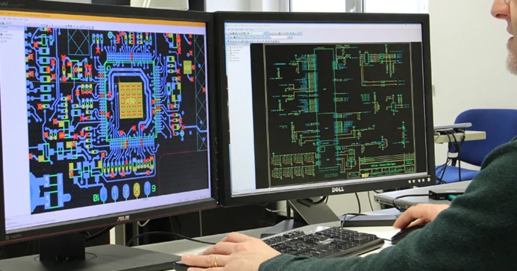
NonDestructive PCB Reverse Engineering | Service
Non-Destructive PCB Reverse Engineering Service Focus Keyphrase Focus Keyphrase: Non-Destructive PCB Reverse Engineering Secondary Keywords: PCB
Recovering Legacy PCBs | Industrial PCB Production & Cloning
PCBs & Industrial PCB Production: Reviving End-of-Life Electronics Focus Keyphrase: PCBs Secondary Keywords: PCB Board,
Locked or Obsolete Chips? We Deliver Practical Decryption Solutions for Your Project
Chip Analysis & Component Verification: Protecting Electronic Devices Manufacturers Focus Keyphrase: Circuit Board Components Secondary
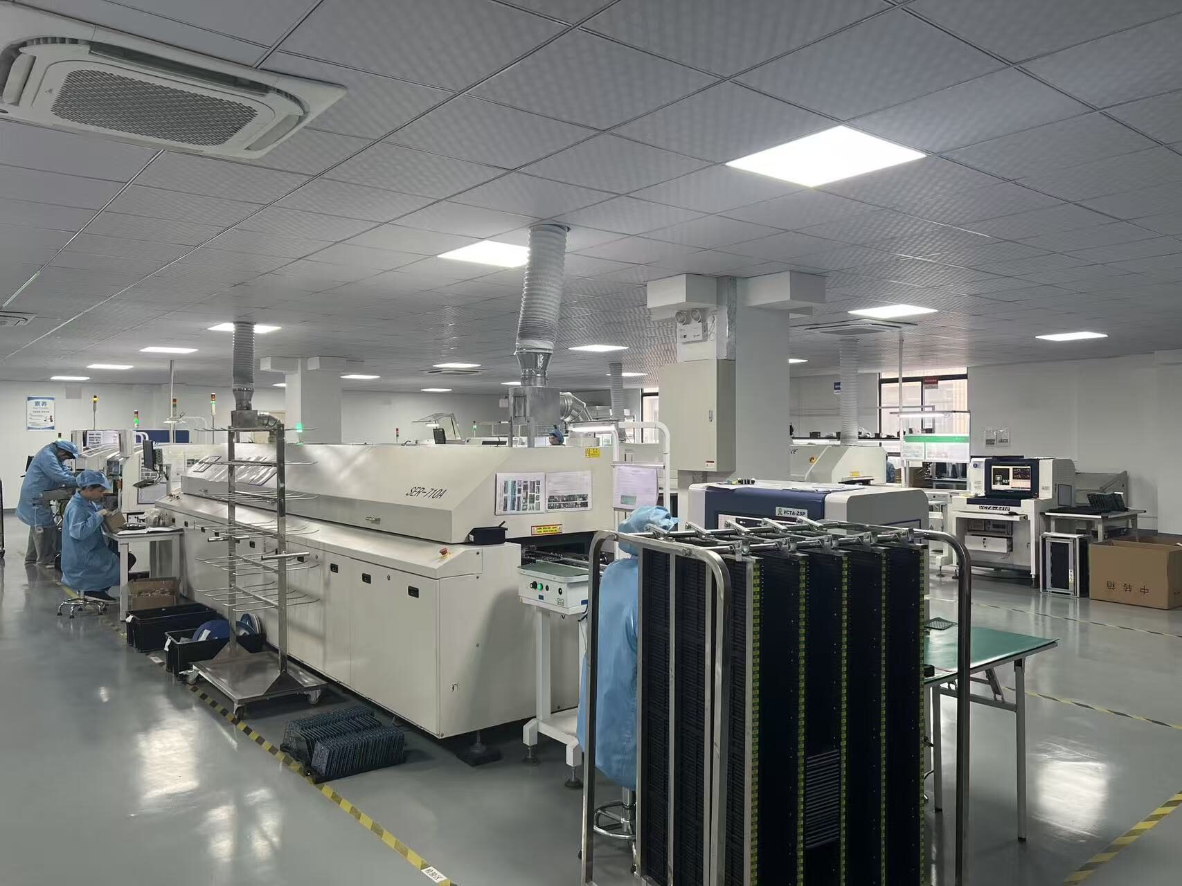
In-House SMT for PCB Board | Direct Printed Circuit Manufacturer
In-House SMT Lines for PCB Board Assembly: Competitive Pricing from a Source Factory Focus Keyphrase:
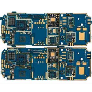
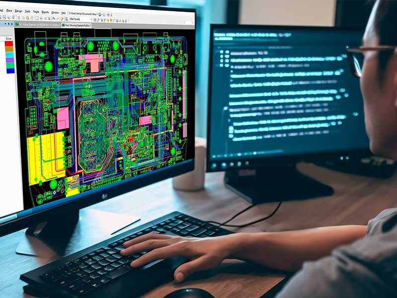
One-Stop PCB Solutions | PCB Design, Layout & Flexible PCB
One-Stop PCB Solutions: From PCB Design to Flexible PCB Fabrication Focus Keyphrase: PCB Design Secondary
Semiconductor Chip Analysis & Security Evaluation | For Microcontrollers
Semiconductor Chip Analysis & Security Evaluation: Engineering Assessment for Microcontrollers Focus Keyphrase: Semiconductor Chip Analysis
SMT Soldering for Electron Devices | Industrial PCB Production
SMT Soldering: Bridging Electron Devices and Circuits for Industrial Production Focus Keyphrase: SMT Soldering Secondary