


Why More Companies Are Backing Up Chip Firmware and Technical Data Before Legacy Equipment Fails
Why More Companies Are Backing Up Chip Firmware and Technical Data Before Legacy Equipment Fails
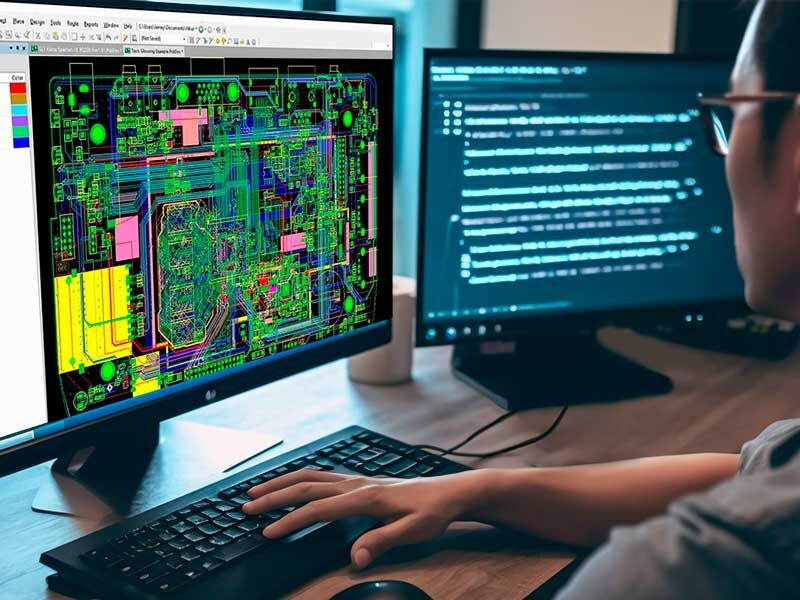
From Non-Destructive Analysis to Mass Production: A Complete PCB Reconstruction Solution
From Non-Destructive Analysis to Mass Production: A Complete PCB Reconstruction Solution In real-world projects, the
PCB Reverse Engineering: Giving New Life to Discontinued Equipment—Our Factory’s Expertise
PCB Reverse Engineering: Giving New Life to Discontinued Equipment—Our Factory’s Expertise With continuous technological advancement,
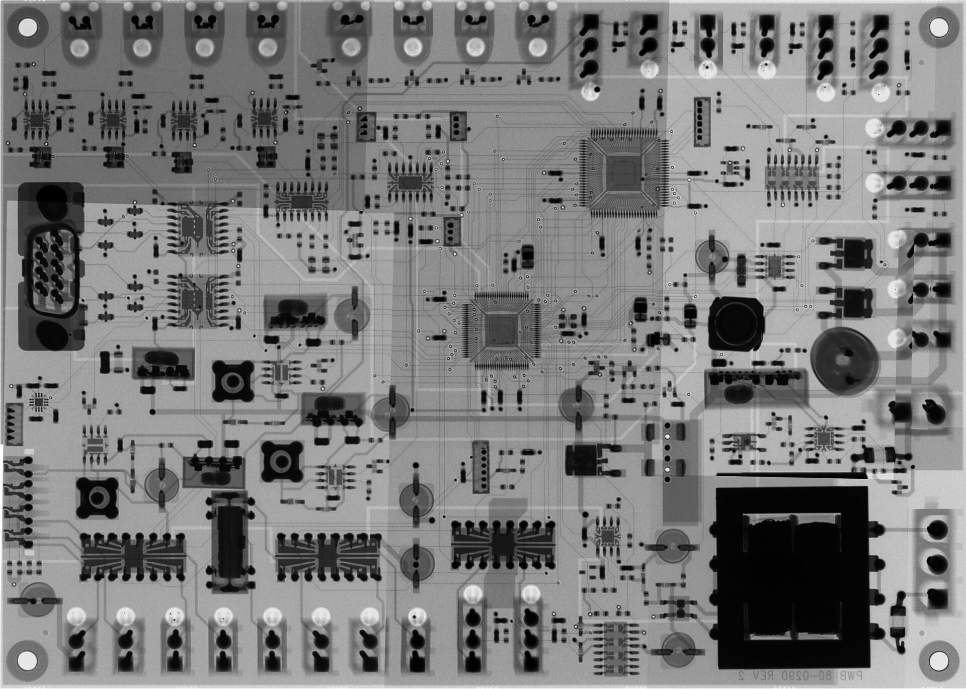
Non-Destructive PCB Analysis & Documentation Recovery Services
Non-Destructive PCB Analysis & Documentation Recovery Services Non-destructive PCB analysis using advanced imaging. Recover schematics,
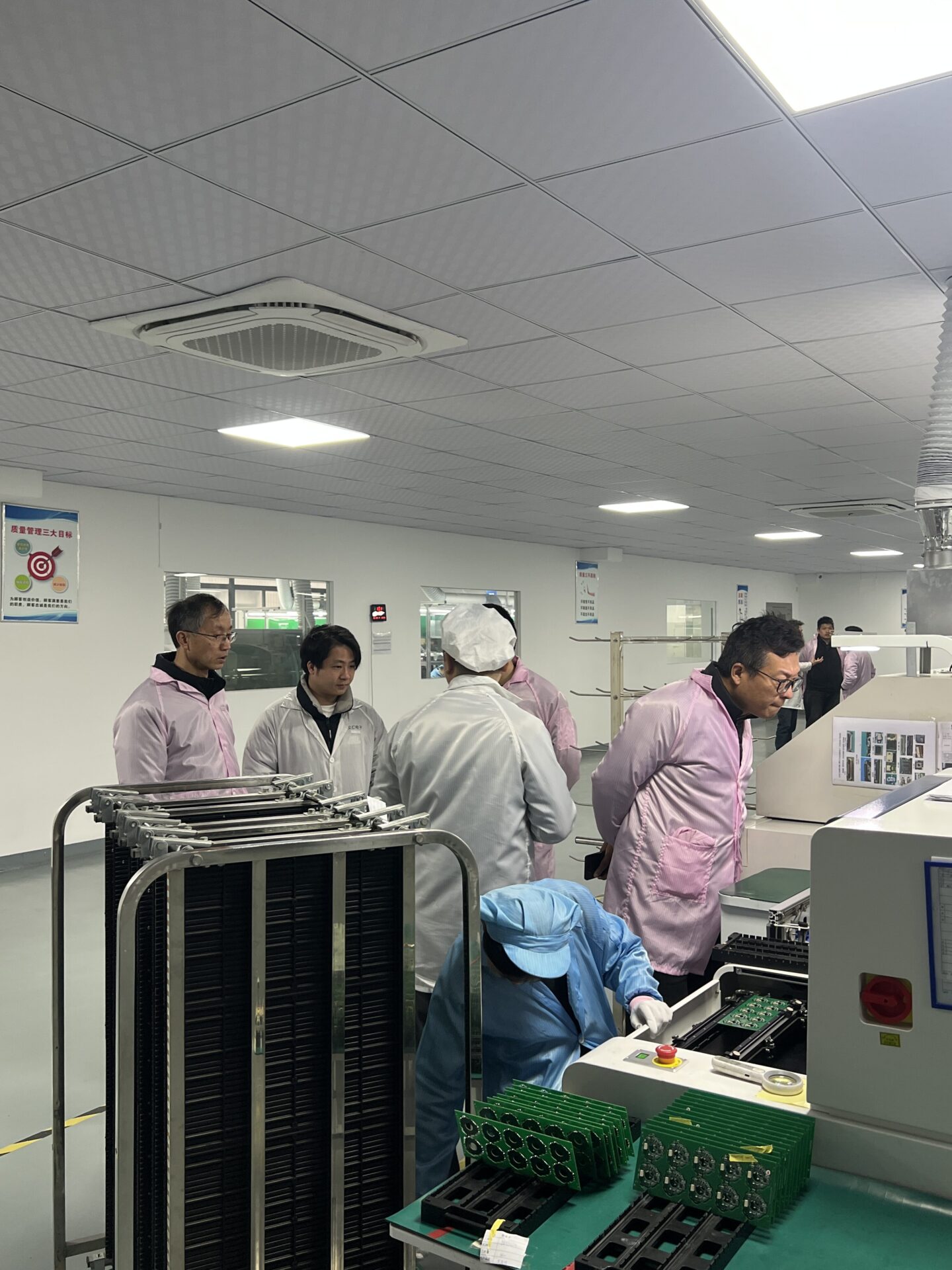
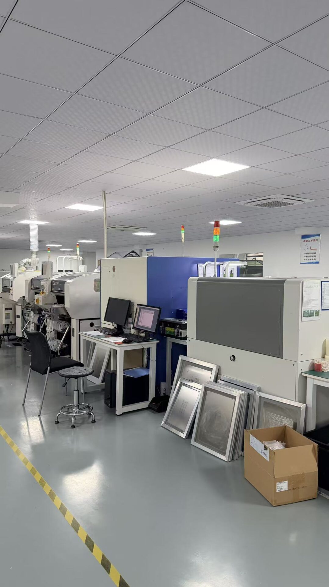
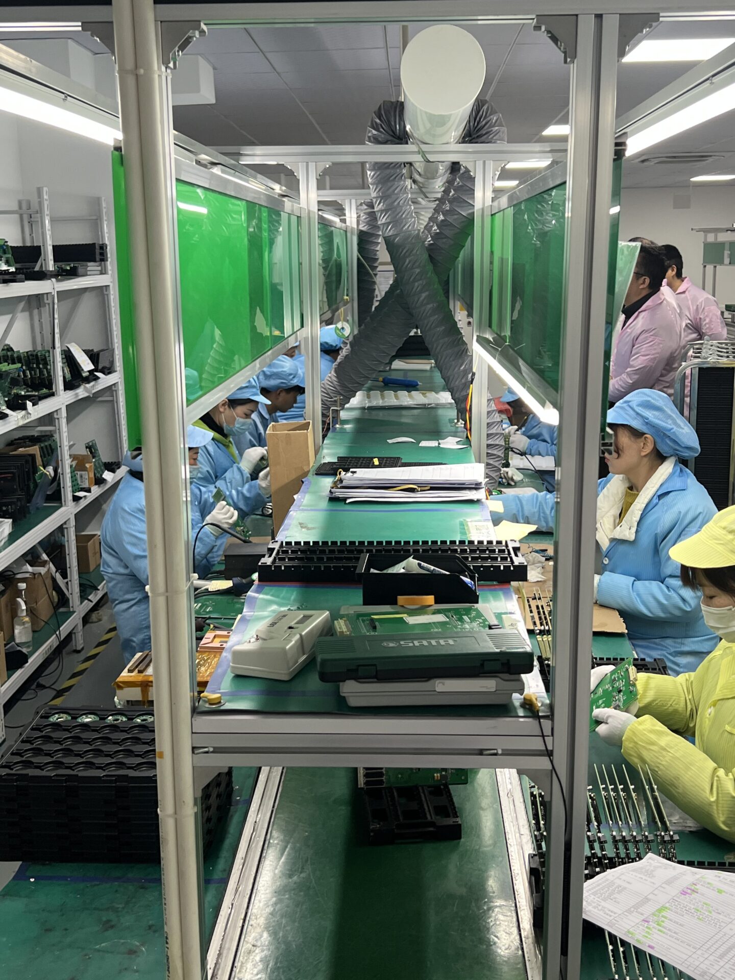
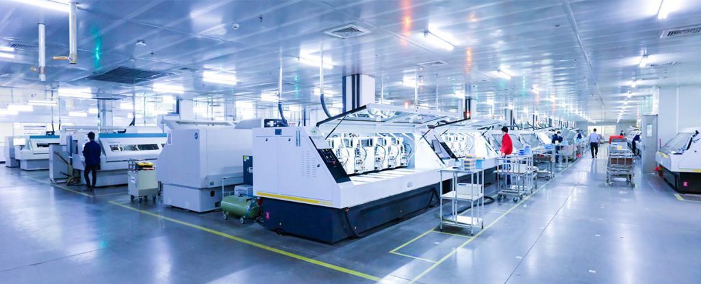
SMT Factory Services | Stable Delivery from Prototype to Mass Production
SMT Factory Services | Stable Delivery from Prototype to Mass Production More Than Assembly —
No Original Files? We Help Clients Rebuild Hardware and Software Systems
No Original Files? We Help Clients Rebuild Hardware and Software Systems In real-world projects, many
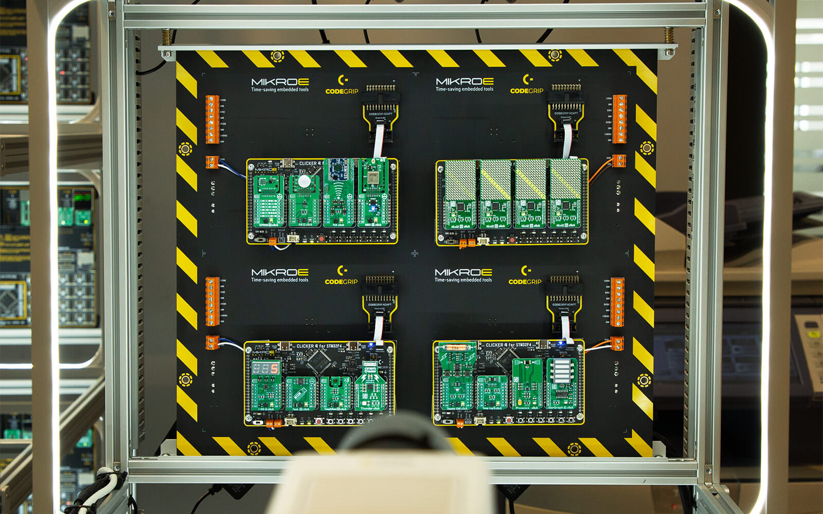
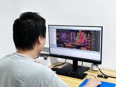
Custom Hardware & Embedded System Design Services: From Concept to Scalable Production
Custom Hardware & Embedded System Design Services: From Concept to Scalable Production 1. Introduction In
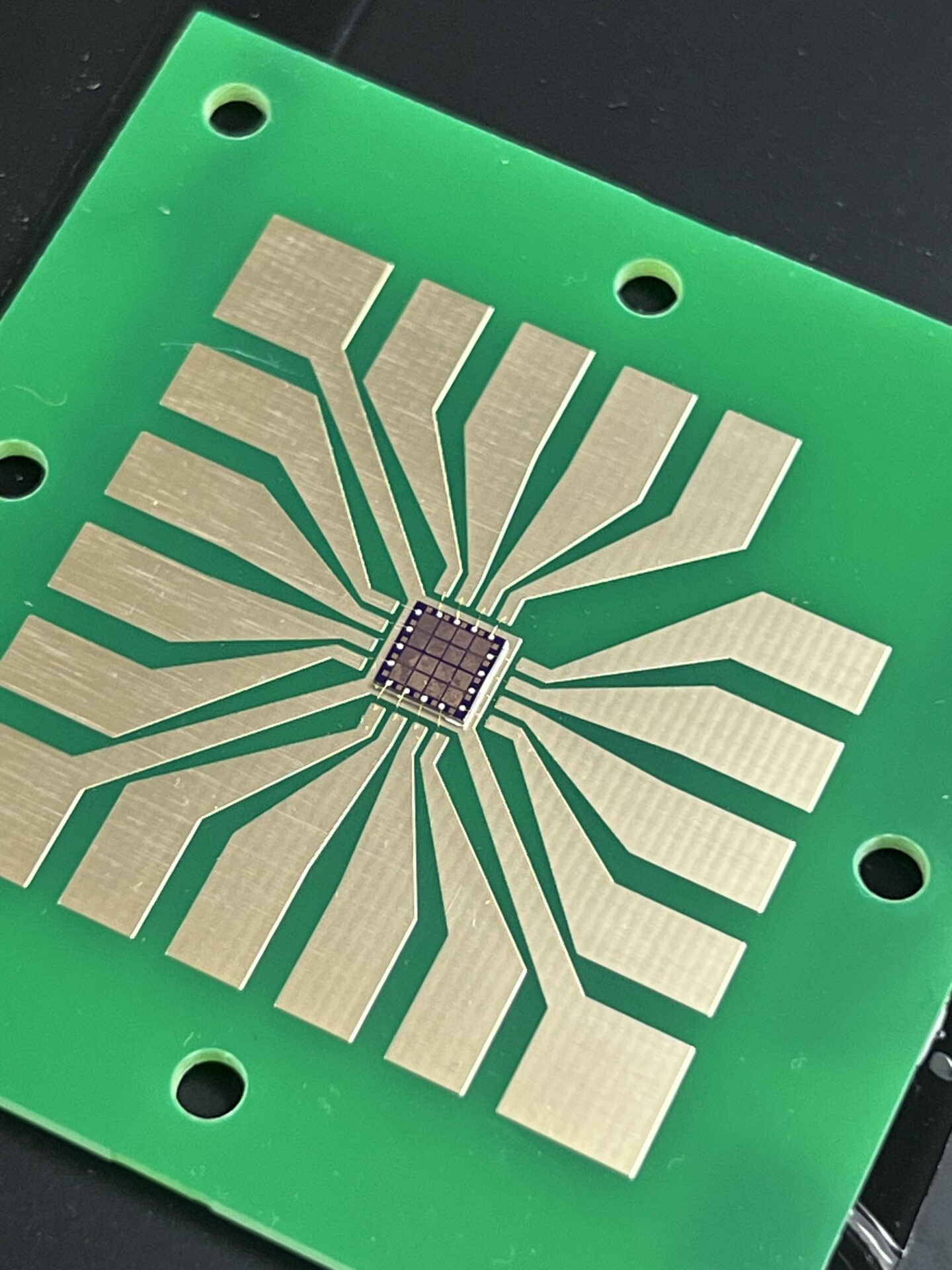
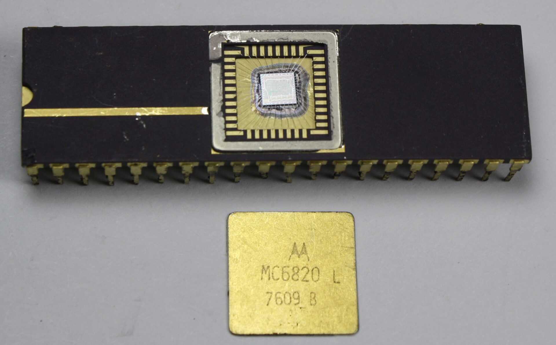
IC Decapsulation & Data Recovery Service (Conversion-Oriented)
IC Decapsulation & Data Recovery Service Professional IC Decapsulation & Data Recovery | In-House Engineering
Struggling with PCB Assembly Mass Production? Here’s What You Need to Know
Why PCB Assembly Fails at Scale Many customers face problems when moving from prototype to