PCB Fabrication Process Explained: From Schematic Design to Finished Board
Focus Keyphrase: PCB Fabrication Process
Secondary Keywords: PCB Layout, Gerber Files, DFM Check, Printed Circuit Board Manufacturing, CAM Engineering.
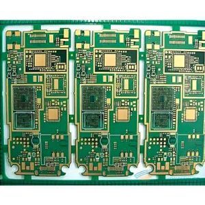
PCB Fabrication is the backbone of the electronics industry. It is the precise engineering process that transforms a digital concept into a physical, functional Printed Circuit Board.
For hardware engineers and product developers, understanding the PCB Fabrication Process is critical. The quality of fabrication directly impacts signal integrity, reliability, and the final yield of Mass Production.
As a direct PCB Fabrication Manufacturer, CtrlcPCB bridges the gap between design and reality. This guide outlines the systematic workflow from Schematic Design to the finished bare board.
1. What Is PCB Fabrication?
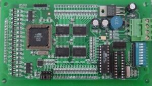
In simple terms, PCB Fabrication is the manufacturing stage where raw copper-clad laminates are etched, drilled, and plated to create the circuit structure. It sits right in the middle of the electronics lifecycle:
Circuit Design (EDA) → PCB Fabrication (Bare Board) → PCB Assembly (PCBA)
It transforms your Gerber Files into the physical foundation for your electronic components.
2. Step-by-Step PCB Fabrication Workflow
Step 1: Schematic Design & Component Selection
Before any physical manufacturing begins, the logic must be defined. Engineers use EDA tools (like Altium, KiCad, or Cadence) to create the Schematic Design.
-
Key Tasks: Defining electrical connections, selecting Electronic Components, and ensuring power integrity.
Step 2: PCB Layout and Routing
Once the schematic is validated, the design moves to physical layout. This is where electrical theory meets manufacturing reality.
-
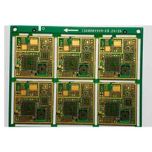
Stack-up Definition: Deciding between a cost-effective 2-layer board or a complex Multilayer PCB.
-
Impedance Control: Routing differential pairs and high-speed signals.
-
Placement: Optimizing component positions for thermal management and DFM (Design for Manufacturability).
Step 3: DRC (Design Rule Check)
The DRC is the final “spell check” for your design. It verifies that your PCB Layout complies with the manufacturer’s capabilities.
-
Typical Checks: Minimum trace width/spacing, via size, and copper-to-edge clearance.
-
Why it matters: Skipping DRC is the #1 cause of fabrication failure and costly re-spins.
Step 4: Generating Gerber Files
The Gerber File is the universal language of PCB Fabrication. It translates your design into a format the factory machines can read. A standard package includes:
-
Copper layers (Top/Bottom/Inner)
-
Solder Mask & Silkscreen layers
-
NC Drill Files (Excellon format)
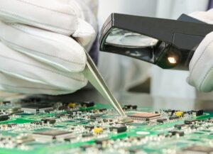
Step 5: CAM Engineering Review (The Factory Gate)
Before we start production at CtrlcPCB, our CAM (Computer-Aided Manufacturing) engineers perform a comprehensive review.
-
We Check For: Open/short circuit risks, acid traps, and solder mask bridges.
-
Optimization: We may add teardrops or adjust line widths to compensate for etching loss, ensuring high yield.
Step 6: Imaging, Etching & Layer Stack-up
-
LDI (Laser Direct Imaging): Transferring the circuit pattern onto the copper.
-
Etching: Chemical baths remove unwanted copper, leaving only your designed traces.
-
Lamination: For Multilayer PCBs, layers of copper and prepreg are bonded together under high heat and pressure.
Step 7: Surface Finish & Profiling
To protect the exposed copper pads and ensure solderability during assembly, a surface finish is applied:
-
HASL: Cost-effective for standard boards.
-
ENIG (Gold): Best for flat surfaces and fine-pitch BGA components.
-
OSP: Organic protection for copper.
Finally, the boards are routed (cut) from the production panel into individual units.
3. Common Fabrication Issues to Avoid
Even the best designs can face manufacturing hurdles. Watch out for:
-
Trace Width/Spacing Violations: Designing below the factory’s minimum capability (e.g., < 4mil) leads to shorts.
-
Poor Pad Design: Incorrect pad sizes cause “Tombstoning” during assembly.
-
Silkscreen Over Pads: Ink on solder pads will prevent proper soldering.
4. Optimization Tips for Engineers
-
Early Supplier Engagement: Confirm stack-up and impedance requirements with your PCB Fabrication Manufacturer before you start routing.
-
Run DFM Checks: Use automated DFM tools to catch manufacturing risks early.
-
Simulation: For high-speed designs, signal integrity simulation prevents performance issues.
5. Conclusion
PCB Fabrication is more than just “printing a board”; it is a precise engineering discipline. A standardized, well-managed fabrication process is the secret to shortening your R&D cycle and reducing total costs.
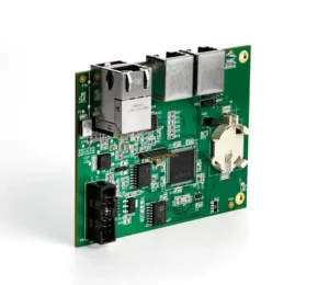
Whether you need rapid PCB Prototyping, reverse engineering analysis, or volume Mass Production, CtrlcPCB provides the engineering support to turn your files into flawless hardware.
🚀 Ready to Fabricate?
Don’t leave your design to chance. Partner with a factory that understands PCB Design and manufacturing.
Get Your Fabrication Quote:
-
Upload Files: Send your Gerber Files for a free CAM review.
-
Technical Support: Talk to our engineers about stack-ups and materials.