IC Substrate
IC Substrate PCBs are important in today’s electronics. You see them in many advanced devices. HUANG TE PCB makes IC Substrate PCBs. We are experts in advanced substrates, making high-quality and reliable products for demanding uses. If you need IC Substrate PCBs, HUANG TE PCB can help.
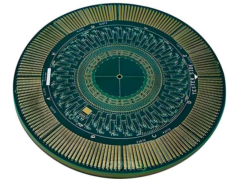
What are IC Substrate PCBs?
Key Characteristics of IC Substrates
In essence, IC substrate PCBs constitute the fundamental basis for advanced IC packaging. Their core function is to establish reliable electrical interconnection between IC chips and conventional PCBs. This role is of paramount importance, as it facilitates the miniaturization of electronic products while accommodating high-density interconnection requirements within devices. It is thus evident that IC substrates are indispensable core components for the development of compact yet high-performance electronic products.
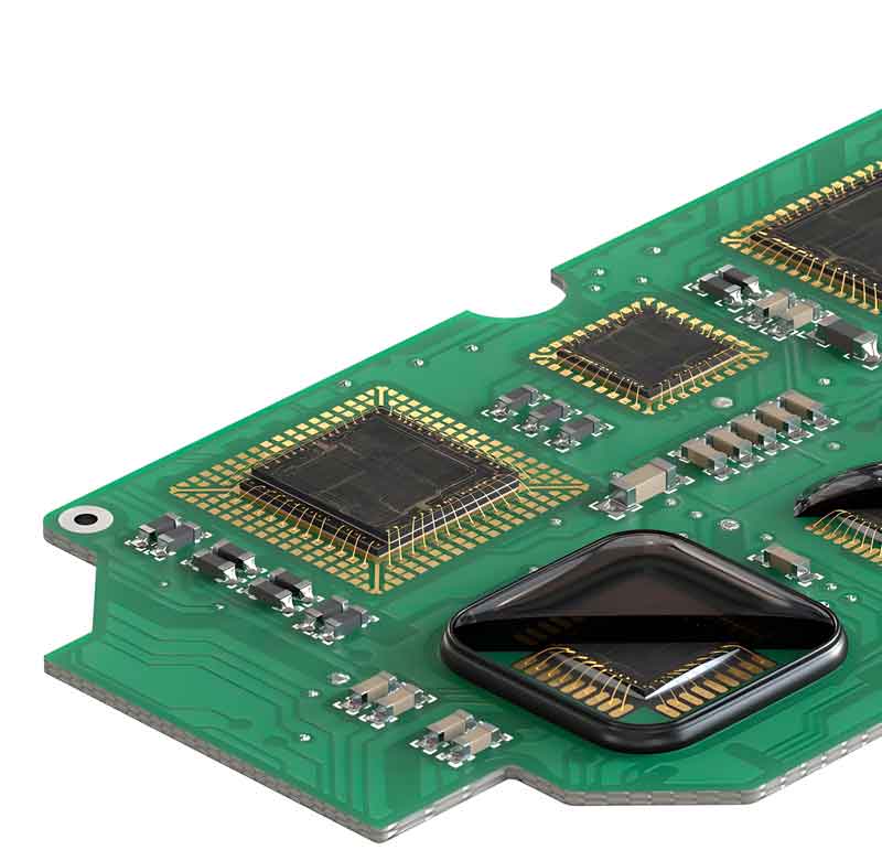
Small Form Factor & Thin Profiles
IC substrates are small and thin. This point is noticeable when you compare them to regular PCBs. They fit in compact devices.
High-Density Interconnections
IC substrates have fine lines and traces with small spaces. This allows many connections in a small area.
Microvias & Advanced Via Technology
IC substrates use microvias, tiny holes made by lasers, to connect layers. Blind and buried vias are used for complex connections.
Material Variety
Many materials are used for IC substrates, for instance, FR4, BT Resin, ABF Resin, Polyimide, and Ceramic. Each material has different properties, depending on the substrate’s use.
Types of IC Substrates We Manufacture
BT Substrate (Bismaleimide Triazine Substrate)
- Made of BT resin.
- Used for mid-to-low-end IC packaging like memory chips and consumer electronics.
- Offers good heat resistance and electrical properties at a lower cost.
ABF Substrate (Ajinomoto Build-up Film Substrate)
- Uses ABF as insulation.
- Best to use in high-end IC packaging such as CPUs, GPUs, and high-speed communication chips.
- Suited for multi-layer, high-density interconnections (HDI). You can incorporate it for advanced packaging.
Ceramic Substrate
- Made of Al₂O₃, AlN, or Si₃N₄.
- Features excellent thermal conductivity and high reliability for high-power IC packaging.
- Used in power devices, RF components, and high-speed communication.
Metal Core Substrate
- Uses aluminum, copper, or stainless steel as the core.
- Offers high thermal dissipation for LED packaging and power devices.
- More cost-effective than ceramic while meeting heat management needs.
Fan-Out Substrate
- Uses Fan-Out Packaging technology.
- Reduces substrate use with Wafer-Level Packaging (WLP), increasing interconnection density.
- Used in high-end smartphone chips, AI chips, and high-performance computing.
High-Frequency Substrate:
- Made from PTFE, LCP, or PI.
- The material serves applications in 5G technology together with millimeter-wave radar systems and high-speed data communication functions.
- It carries low dielectric constant (Dk) and low dielectric loss (Df) for signal transmission.
BGA Substrates | Ball Grid Array: BGA substrates are incorporated for ICs with many pins. Is performance is also impeccable.
CSP Substrates | Chip Scale Package: CSP substrates are very small, almost chip-sized, for devices with limited space.
MCM Substrates | Multi-Chip Module: MCM substrates integrate multiple chips in one package for better system integration.
FC Substrates | Flip Chip: FC Substrates allow direct chip attachment, improving performance.
Rigid IC Substrates: Rigid IC substrates present strength and cost efficiency that fits many application needs.
Flexible IC Substrates: Flexible IC substrates allow bending when applications demand flexible substrates.
Ceramic IC Substrates: Ceramic IC substrates manage heat well for high-power applications.
HUANG TE PCB's IC Substrate PCB Manufacturing Capabilities
| Items | Content |
|---|---|
| Subtractive Process (SP) | We use subtractive etching for IC substrates. This is standard. |
| Modified Semi-Additive Process (MSAP) | We are MSAP experts. This process makes finer lines and higher density. |
| Additive Process (AP) | We use additive processes for very fine features, if needed. |
| Cutting-Edge Technology & Equipment | We use advanced equipment like laser drilling for microvias, precision etching, and plating lines. This technology makes precise IC substrates. |
| Material Expertise | We work with many IC substrate materials, incorporating FR4, Polyimide, BT/ABF resins, and Ceramics. Our engineers can help you with material selection. |
| High Layer Count & Design Complexity | We make multi-layer IC substrates with complex designs, handling fine pitches and routing. |
Applications of IC Substrate PCBs
Telecommunications
For fast networks and communication devices like servers and networking gear.
High-Speed Computing & Data Centers
To support processors and memory in data centres
Consumer Electronics
For compact, powerful devices like smartphones and wearables.
Automotive Electronics
In cars for ADAS and infotainment systems.
Medical Devices
For reliable medical equipment.
Industrial Control Systems
For automation in factories
LED Lighting
For advanced LED lights and heat management
RF and Microwave Applications
To support high-frequency signals
Automated Optical Inspection (AOI)
We use AOI to check for visual problems automatically.
Results
We use AXI to check inside layers for hidden issues.
Electrical Testing
We test circuits electrically to ensure they work.
Impedance Control
We control impedance for high-speed signals to maintain signal quality.
Certifications and Standards
HUANG TE PCB is certified to ISO 9001, ISO 14001, and IATF 16949 and follows RoHS and IPC standards.
Material Traceability & Quality
We use high-quality, traceable materials.
The values we live by
Viverra maecenas accumsan lacus vel. Risus ultricies tristique.
HUANG TE PCB
Why Us
- Extensive Experience & Expertise
- Advanced Technology & Equipment
- Uncompromising Quality & Reliability
- Customization & Design Support
- Competitive Pricing
- On-Time Delivery
- Dedicated Customer Support